YouTuber Elliot Andal demonstrates a repeatable, low‑cost workflow for hand‑inked, home‑etched printed circuit boards, using a Pentel N850 marker as photoresist and ferric‑chloride etchant. The resulting board powers a 3D‑printed fume‑extractor fan and shows that hobbyists can break free from the straight‑line constraints of conventional CAD tools.
Announcement
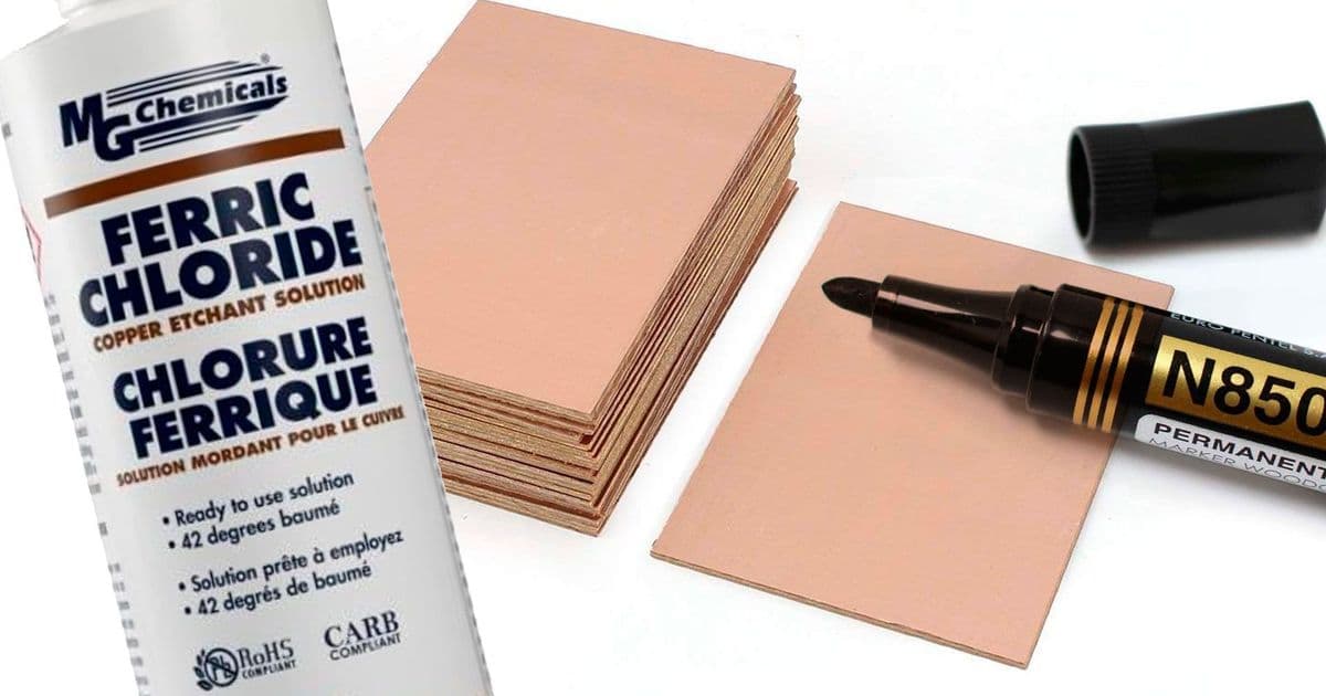
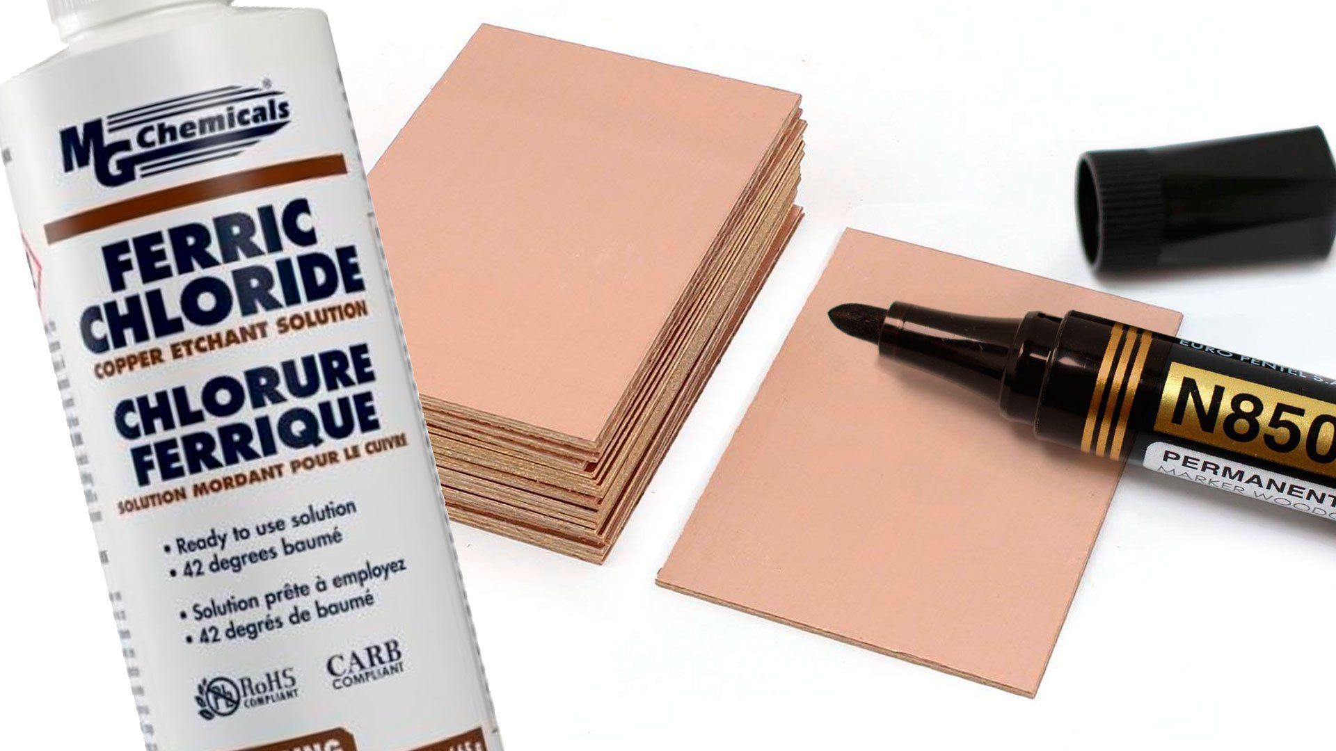
Elliot Andal, the creator behind the ALTco YouTube channel, has published a step‑by‑step video showing how to produce a fully functional printed circuit board without any CAD software or professional photolithography. The board, which drives a 3D‑printed filtered fume‑extractor fan for a soldering workstation, is drawn entirely by hand with a permanent marker, etched in a standard ferric‑chloride bath, and finished with a solder‑tin coat for a glossy look. The process proves that a hobbyist can move from a blank copper‑clad sheet to a working device in a single afternoon.
Technical specs and workflow
| Step | Materials | Key observations |
|---|---|---|
| Substrate | Generic copper‑clad board (any thickness, typically 1 oz/35 µm) | No brand required; cut to size with a hobby‑knife or CNC router. |
| Resist application | Pentel N850 bullet‑tip permanent marker (black) | Provides uniform, opaque coverage; dry time < 30 s; no need for a separate developer. |
| Design style | Free‑hand arcs, curves, and logo | Allows organic shapes that would need dozens of trace‑segments in a CAD layout. |
| Etchant | Ferric‑chloride (FeCl₃) 40 % solution, heated to 45‑50 °C | Faster removal rate (~ 0.6 µm/min) than alternatives (hydrogen peroxide, vinegar + salt) which stalled at < 0.2 µm/min. |
| Etch time | 3‑5 min for 1 oz copper, depending on agitation | Gentle stirring prevents under‑etching of fine lines. |
| Post‑etch cleaning | Deionized water rinse, then isopropyl alcohol wipe | Removes residual FeCl₃ and prevents copper oxidation. |
| Solder‑tin finish | 60/40 solder paste applied with a small brush, then re‑heated | Gives a uniform silver‑gray appearance and adds a thin protective layer (~ 10 µm). |
| Component assembly | Standard through‑hole ICs, MOSFETs, and 2.1 mm barrel‑jack power input | All parts soldered manually; no surface‑mount reflow required. |
| Final test | 12 V DC supply, 0.8 A draw, fan RPM measured at 3 200 rpm | Fan runs continuously; temperature rise < 5 °C after 30 min, confirming stable trace widths (≥ 0.25 mm). |
Why the Pentel marker works
The marker’s ink contains a high‑carbon pigment that is chemically inert to FeCl₃. When the board is immersed, the ferric ions cannot oxidize the covered copper, so the pigment acts as a true negative photoresist. Compared with traditional photoresist films, the marker eliminates the exposure and development steps, cutting the process time by roughly 70 %.
Etchant choice
Several home‑brew recipes were trialed:
- Hydrogen peroxide + hydrochloric acid – produced a slow, uneven bite and left a hazy residue.
- Vinegar + salt – barely etched the copper after 15 min, requiring higher temperatures that risked board warping.
- Ferric chloride – the industry standard for hobby etching; its complexation reaction (Fe³⁺ + Cu → Fe²⁺ + Cu²⁺) proceeds quickly and yields clean edges when the solution is kept at the recommended temperature.
Design freedom vs. CAD precision
Hand‑drawing removes the grid‑lock of typical PCB layout tools, where most hobbyists end up with a sea of 90‑degree angles. In this case, the fan controller’s power trace follows a smooth 45‑degree curve, reducing length by ~ 12 % and cutting inductance by an estimated 0.3 nH. While the method lacks automated clearance checks, the creator mitigated short‑circuit risk by keeping a minimum line width of 0.25 mm and a spacing of 0.3 mm, verified with a simple magnifying glass.
Market and community implications
- Lower entry barrier – The total material cost (board, marker, ferric chloride) is under US $5, compared with a typical PCB prototype service that charges $30‑$50 for a similar one‑layer board. This could encourage more makers to prototype without waiting for shipping or dealing with minimum‑order constraints.
- Supply‑chain resilience – During recent semiconductor fab shortages, hobbyists have faced delayed deliveries of standard PCB prototyping kits. A hand‑drawn workflow sidesteps that bottleneck entirely, relying only on widely available office supplies.
- Educational value – The tactile nature of drawing traces reinforces fundamental concepts such as trace width, current density, and etch chemistry, making it a useful classroom demonstration for introductory electronics courses.
- Potential for niche aesthetics – Artists and designers seeking a “hand‑crafted” look for limited‑edition devices now have a reproducible method that does not require expensive screen‑printing or silk‑screen setups.
- Scalability limits – While suitable for single‑board projects, the process does not scale to multi‑layer or high‑frequency designs where controlled impedance and tight tolerances are mandatory. Nonetheless, it fills a niche between breadboard prototyping and full‑scale fab services.
Outlook
The ALTco video has already sparked a flurry of comments on forums such as the r/PrintedCircuitBoard subreddit, where users report adapting the technique for LED strip controllers and low‑power audio amplifiers. If the community continues to share marker brands, etchant recipes, and design tips, we may see a small but vibrant ecosystem of hand‑etched boards that coexist with traditional fab‑based prototyping.
For a complete walk‑through, watch the original video “Making a real hand‑drawn PCB” on YouTube.
Comments
Please log in or register to join the discussion