
Cadence Design Systems has successfully brought up its first system chiplet silicon, marking a pivotal step in the shift toward modular, chiplet-based designs for physical AI applications. This innovation addresses the challenges of scaling beyond Moore's Law by enabling heterogeneous integration and high-speed memory operations across chiplets. For developers and engineers, this could significantly accelerate the creation of efficient, power-optimized systems for edge and autonomous technologie
Cadence's System Chiplet Silicon Breakthrough: Paving the Way for Modular Physical AI Architectures
In a significant leap for semiconductor design, Cadence Design Systems has announced the successful silicon bring-up of its first system chiplet. This development, detailed in a recent Forbes article by Marco Chiappetta, underscores the company's push toward a chiplet ecosystem that could redefine how we build complex System-on-a-Chip (SoC) platforms, particularly for physical AI applications like autonomous driving and edge computing.
The Rise of Chiplet Architectures
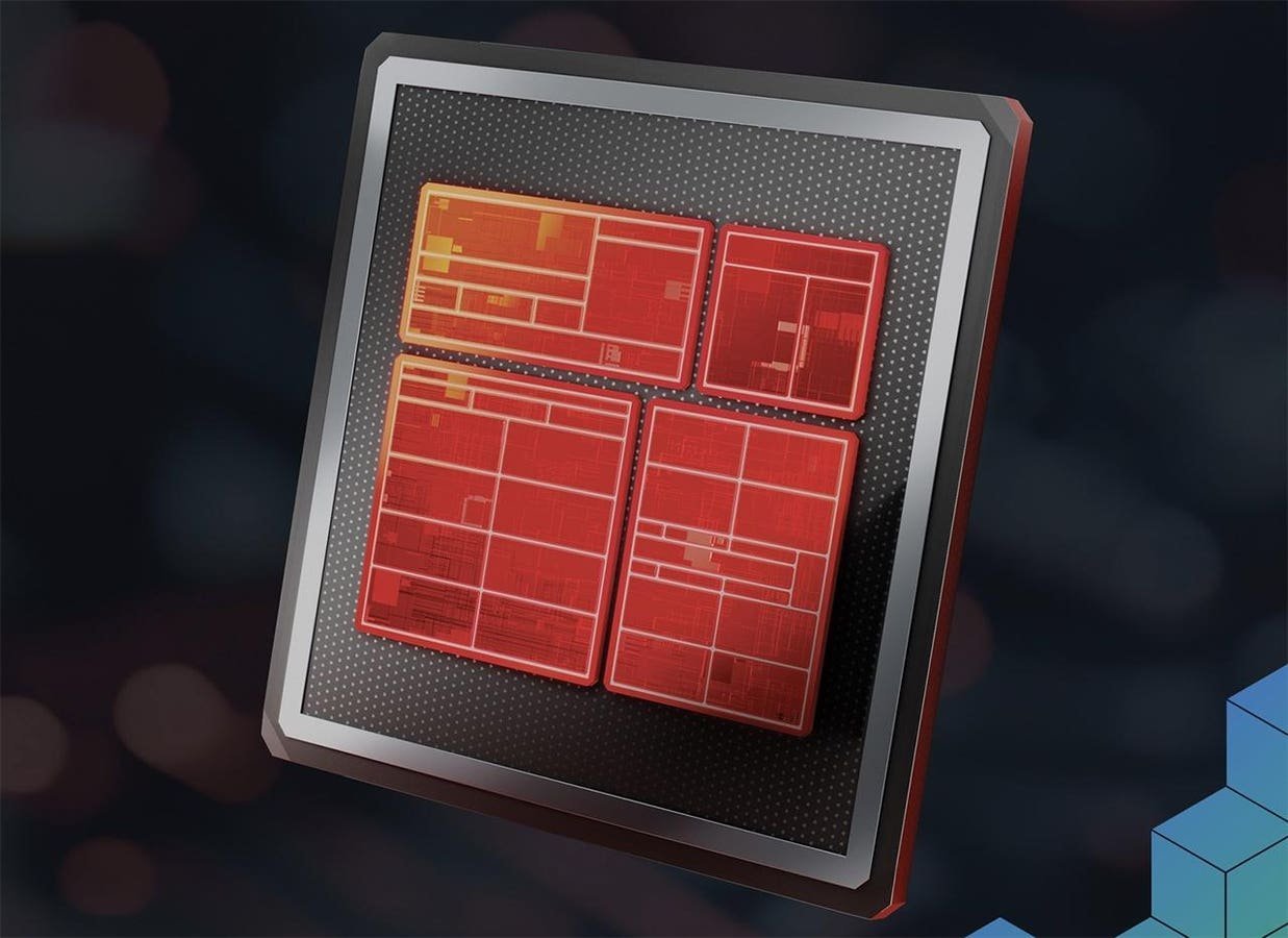
As Moore's Law begins to falter and the costs of advanced manufacturing soar, the semiconductor industry is increasingly turning to chiplet-based designs. These modular approaches allow engineers to combine diverse components—such as processors, memory interfaces, and accelerators—from different process nodes into a single, cohesive system. Cadence's system chiplet serves as the 'backbone' for this integration, incorporating essential elements like a system processor, safety management processor, various controllers, a Network on Chip (NoC), and Cadence PHY IP for LPDDR5 memory. All these are interconnected via UCIe (Universal Chiplet Interconnect Express), an emerging standard for die-to-die connectivity.
The real-world validation of this architecture is impressive. Cadence achieved stable initialization of LPDDR5X memory at 9,600 MT/s across chiplets, even pushing speeds into the mid-teens under stress conditions. Additionally, UCIe was demonstrated at 32 Gb/s over a 25 mm link, with successful boot-up, memory training, and system discovery—all in actual silicon, not just simulations. This isn't theoretical; it's a proven foundation that tackles timing, signal integrity, and synchronization hurdles head-on.
Why This Matters for Physical AI
Physical AI systems, which power everything from robotics to self-driving cars, demand immense computational resources and memory bandwidth while operating under stringent constraints on power, thermal management, and form factor. Traditional monolithic SoCs struggle here, as they require fabricating everything on a single, expensive die. Chiplets, however, enable designers to optimize each module independently—using the best process node for compute-heavy accelerators or power-efficient I/O—while improving yield and reducing time to market.
Cadence's system chiplet aligns perfectly with these needs. By validating high-speed memory operations and UCIe interoperability, it provides a robust reference for developers building next-generation embedded and edge-AI systems. Imagine accelerating the development of autonomous vehicles where safety-critical processors and AI accelerators can be mixed and matched without the risks of a full custom SoC redesign.

Industry Implications and Challenges
This milestone validates Cadence's strategy and could shorten design cycles for semiconductor teams exploring multi-die solutions. As a major EDA and IP provider, Cadence is positioning itself as a key enabler in the chiplet ecosystem, potentially driving broader adoption across AI accelerators, custom I/O, and domain-specific processors. The use of UCIe also signals alignment with industry standards, fostering multi-vendor interoperability that could lower barriers for innovation.
Yet, the path forward isn't without hurdles. Advanced packaging and interconnects introduce new complexities in cost, supply chains, thermal management, and heterogeneous integration—especially critical in edge environments where reliability is non-negotiable. Cadence faces stiff competition from other players advancing their own chiplet strategies, so success will hinge on ecosystem partnerships, customer wins, and proven economics.
For developers, this means a tangible reference platform to de-risk projects. Instead of starting from scratch, teams can leverage Cadence's silicon-proven design to validate assumptions early, potentially saving millions in R&D. In physical AI domains, where every watt and millimeter counts, this modularity could be the difference between a viable product and an over-engineered failure.
A Milestone in Modular Silicon
Cadence's system chiplet isn't just another piece of silicon—it's a maturation point for an industry in transition. As edge and physical-AI markets explode, this platform could empower designers to craft tailored, efficient architectures that were previously cost-prohibitive. Whether it sparks a wave of commercial adoptions or becomes a cornerstone for collaborative innovation, one thing is clear: Cadence has laid a solid foundation for the modular future of semiconductors, inviting engineers to build smarter, faster, and more reliably.
Comments
Please log in or register to join the discussion