MSI's $5,000 flagship GPU cracked under thermal shock when pushed beyond limits with 2,500W XOC BIOS
Extreme overclocking attempts with MSI's flagship RTX 5090 Lightning Z ended in disaster when the $5,000 GPU cracked under thermal shock during a record-breaking run. The incident highlights the razor-thin margins between pushing hardware to its absolute limits and catastrophic failure.
The $5,090 Overclocking Beast
MSI's RTX 5090 Lightning Z represents the pinnacle of extreme overclocking hardware, featuring dual 12V-2x6 power connectors capable of drawing up to 1000W each through a 40-phase VRM. The card ships with a special 2,500W XOC BIOS specifically designed for liquid nitrogen cooling scenarios, along with an 8-inch display replacing the traditional backplate for real-time telemetry monitoring.
Initial Success Before Catastrophe
YouTuber Alva Jonathan, who had been consulting with MSI Taiwan on the GPU's development since August 2025, began testing with more modest overclocks. Starting at 3.25 GHz with 1.05V voltage, the card consumed over 700W and achieved 43,112 points in 3DMark Port Royal - significantly higher than the typical 36-37K points regular RTX 5090 cards achieve.
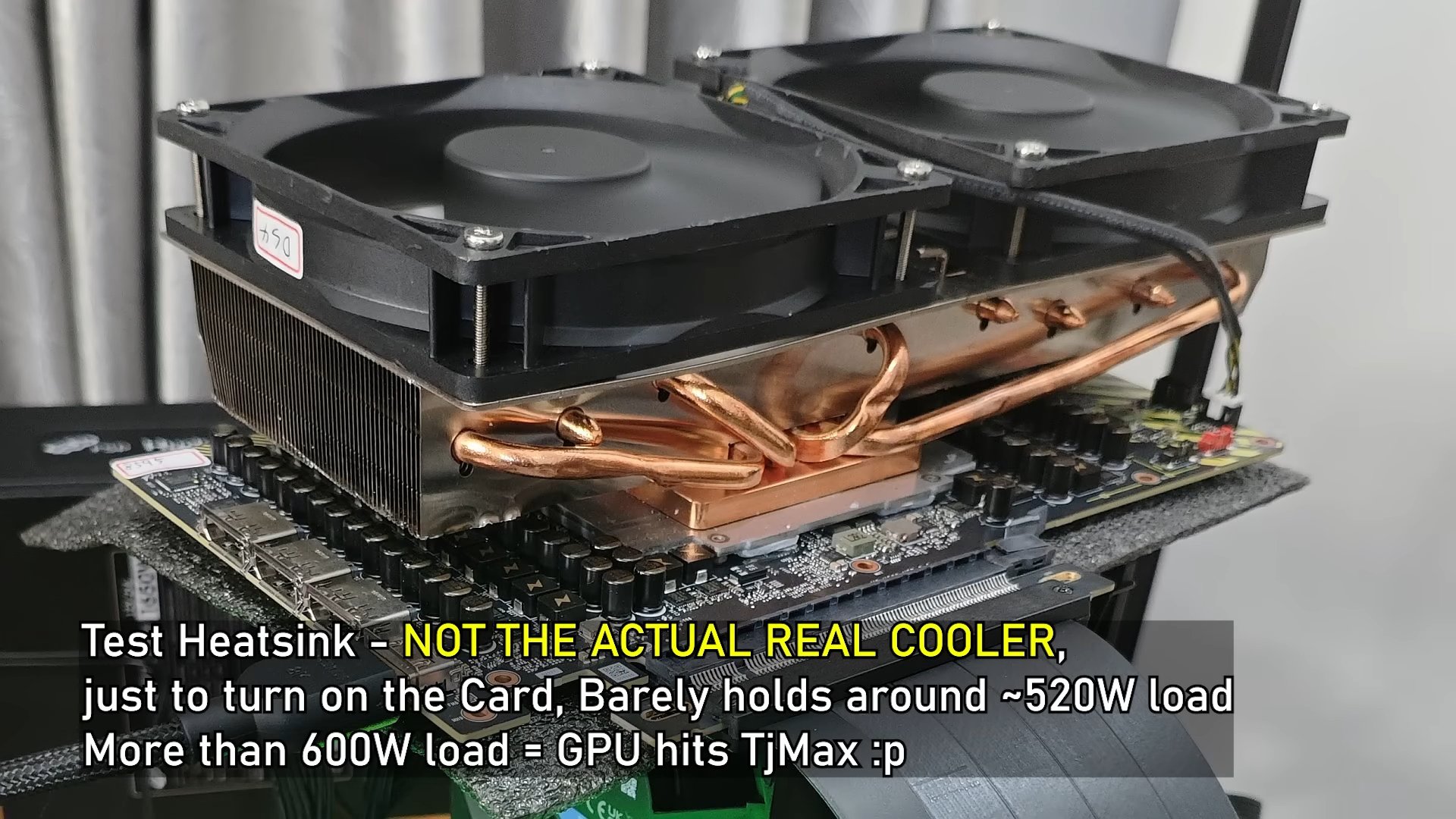
The GPU maintained balanced power distribution between its two 16-pin connectors, maxing out at 772W during these initial runs. However, the real testing began when Jonathan moved to ARX's liquid nitrogen facilities.
Liquid Nitrogen Challenges
Even with LN2 cooling, maintaining stable operation proved difficult. The heatsink contacting the GPU core reached -40 degrees Celsius, while the GPU itself remained at positive temperatures, climbing to 9 degrees under full load. At 1.12V and 3.42 GHz boost clocks, the card consumed over 1,000W.
Temperature management became critical as the safe operating range for high-voltage LN2 overclocking sits between 0 and 15 degrees. When temperatures hit 21 degrees during one run, the system immediately crashed. However, GPUPI benchmarks proved more forgiving, allowing Jonathan to push clocks to 3.6 GHz at around 0 degrees.
The team eventually settled on 3.5 GHz as their optimal operating point, successfully breaking the world record for highest HWBot score in Geekbench 5 with 683,433 points - a record that still stands.
The Fatal Thermal Shock
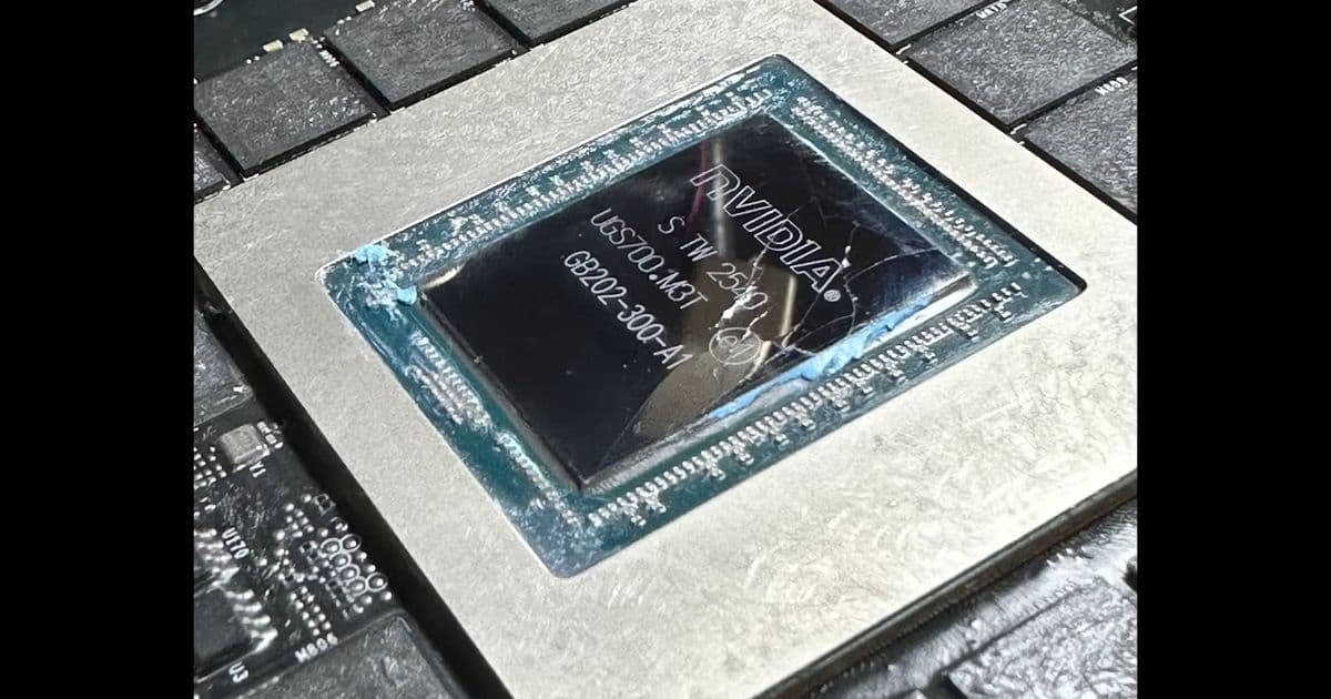
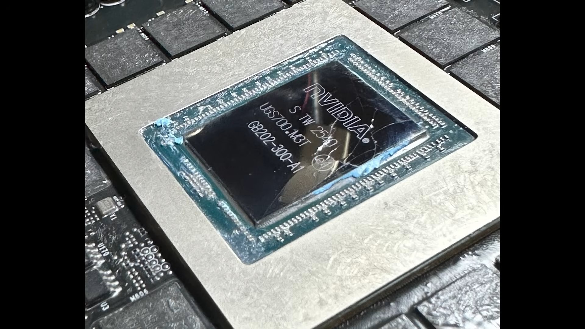
The disaster struck when attempting to use the 2,500W XOC BIOS. Jonathan was working with an earlier revision that pushed excessive voltage to the GPU core too quickly. At just 1.2V - a voltage considered safe for negative temperatures under LN2 - the GPU core cracked visibly.
Understanding Thermal Shock Failure
The failure mechanism involved a severe temperature imbalance across the GPU die. While portions of the core remained cold from LN2 cooling, other areas had become hotspots, creating internal stress that the silicon couldn't withstand. This thermal shock caused the core to crack, rendering the $5,000 card unusable.
Recovery and Future Attempts
Despite losing one sample, Jonathan maintains four additional PCBs for continued testing. The damaged card isn't completely dead - it can potentially be revived using a donor GPU core since the surrounding components remain intact.
Future attempts will likely involve using a more stable retail BIOS and implementing better cooling solutions with more secure mounting to prevent similar thermal stress issues. Jonathan also noted the need for improved cooling infrastructure to tackle other world records like 3DMark Solar Bay Extreme.
This incident serves as a stark reminder of the extreme engineering challenges in pushing modern GPUs beyond their designed limits, where even small voltage increases or temperature imbalances can result in catastrophic hardware failure.
Comments
Please log in or register to join the discussion