A Japanese engineer leveraged Google's Gemini AI to design a functional x86-compatible motherboard around NEC's V30 processor, demonstrating both the potential and current limitations of AI in hardware design workflows.
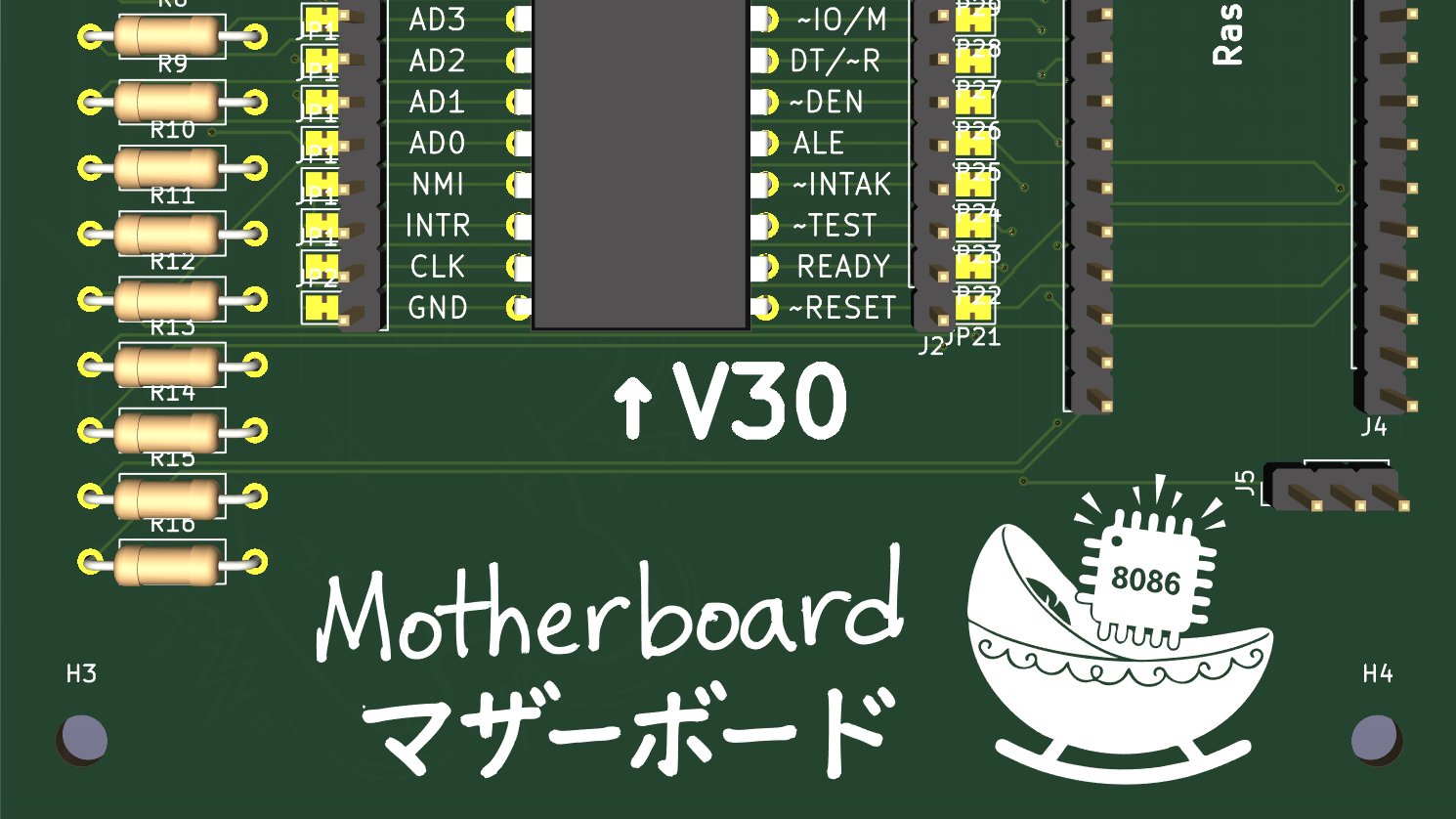
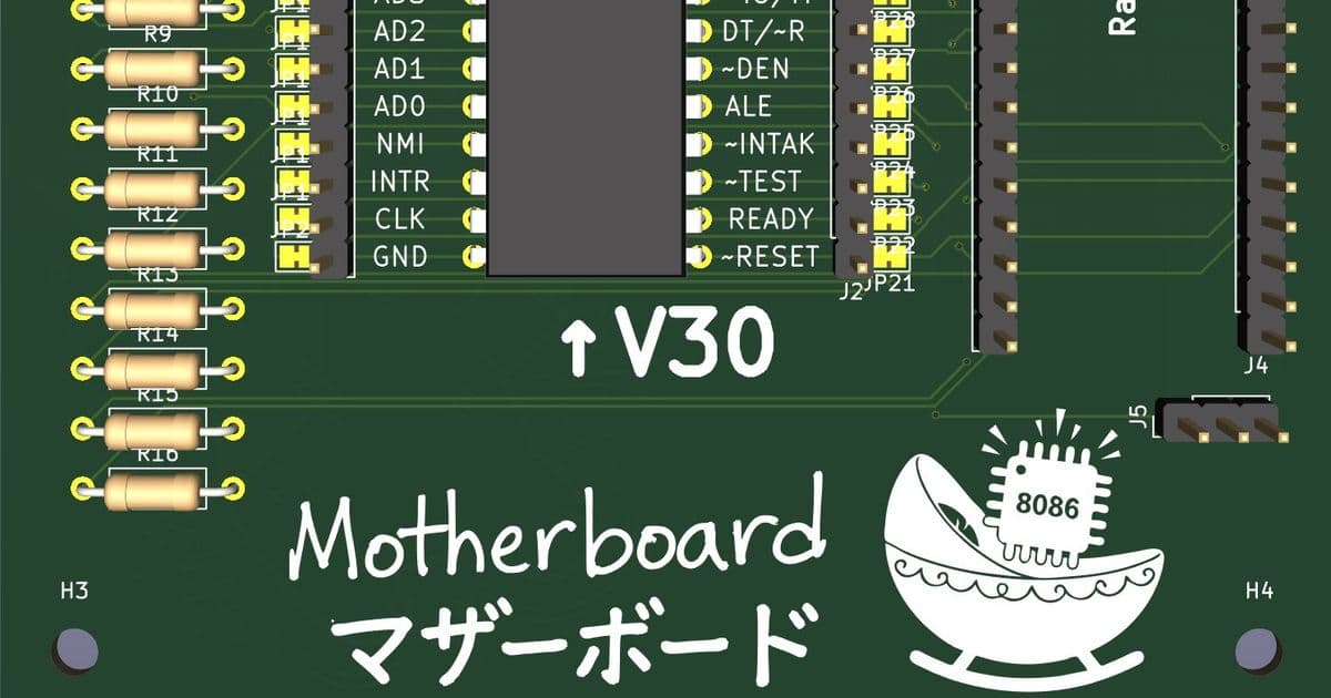
Japanese hardware engineer Ikejima has successfully designed a functional x86-compatible motherboard using Google's Gemini AI as a collaborative design partner. The project centered on NEC's V30 processor—a 1980s-era clone of Intel's 8086 CPU—implemented through a custom "cradle" architecture based on Raspberry Pi's RP2040 microcontroller. This hybrid human-AI approach provides valuable insights into the evolving role of artificial intelligence in semiconductor design pipelines.
Technical Implementation and Specifications
 The V30 processor (μPD70116) operates at 5V logic levels while interfacing with the 3.3V RP2040 microcontroller, creating immediate voltage translation challenges. Ikejima employed Gemini to generate circuit designs in KiCad using Python scripting automation, significantly accelerating schematic capture. The RP2040's dual-core architecture proved essential: Core 0 managed V30 communication while Core 1 handled USB debugging interfaces, preventing clock synchronization issues that derailed Ikejima's earlier 8088 implementation attempt.
Gemini generated C++ firmware using the Pico SDK to implement three critical functions:
- Memory emulation allocating 128KB of the RP2040's 264KB SRAM as V30 address space
- An x86 assembler/disassembler for program loading
- Real-time debugging protocols
The AI also designed the memory subsystem architecture, though this revealed critical limitations. Gemini's schematic proposal overlooked the 8086's multiplexed address/data bus architecture, where AD0-AD15 pins carry both address and data signals across consecutive clock cycles. This resulted in a dangerous short-circuit condition during initial testing that would have damaged components without the USB port's overcurrent protection.
Manufacturing and Debugging Realities
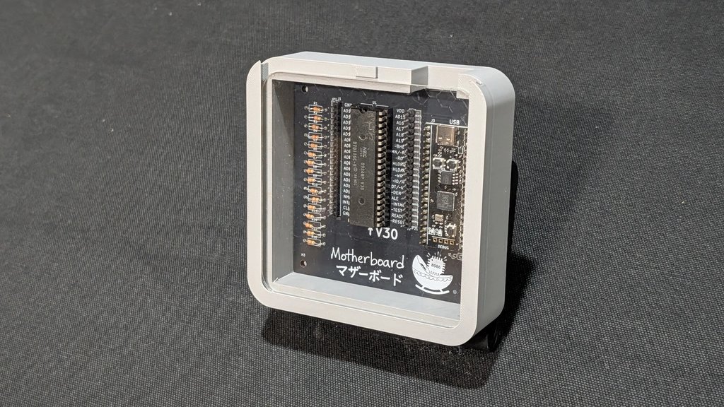 Post-manufacturing validation exposed another oversight: Gemini's memory controller failed to implement the 8086's even/odd byte banking scheme requiring separate memory chips. Ikejima resolved this by manually rewriting memory-access routines after logic analyzer analysis showed corrupted data pathways. Final validation occurred through successful execution of MS-DOS's COMMAND.COM via Hirofumi Iwamoto's HI-DOS BIOS implementation, though storage limitations prevented full disk emulation.
Market Implications for AI-Assisted Design
This project demonstrates AI's current hardware design capabilities:
- Acceleration Potential: Gemini reduced weeks of work on assembler/disassembler tools to hours
- Cost Efficiency: The entire BOM cost ~$15 (V30: $2; RP2040: $1; PCB: $12)
- Limitations: AI cannot interpret physical constraints like voltage tolerances or bus contention risks
Semiconductor analysts note that while AI can automate routine coding and schematic tasks, human oversight remains essential for:
- Physical layer validation
- Power integrity analysis
- Timing closure verification
Major EDA vendors (Cadence, Synopsys) now integrate AI co-pilots, but Ikejima's hands-on experiment reveals these tools remain assistants rather than replacements. As chip complexity increases with 3nm/2nm nodes, AI's role in reducing design iteration cycles grows—but catastrophic failures like bus contention incidents underscore why human expertise stays irreplaceable for physical implementation.
 Bruno Ferreira is a contributing writer with expertise in semiconductor architectures and embedded systems.
Comments
Please log in or register to join the discussion