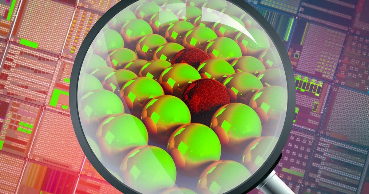
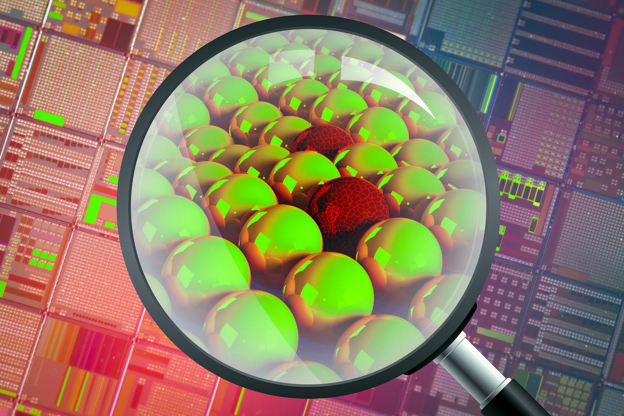
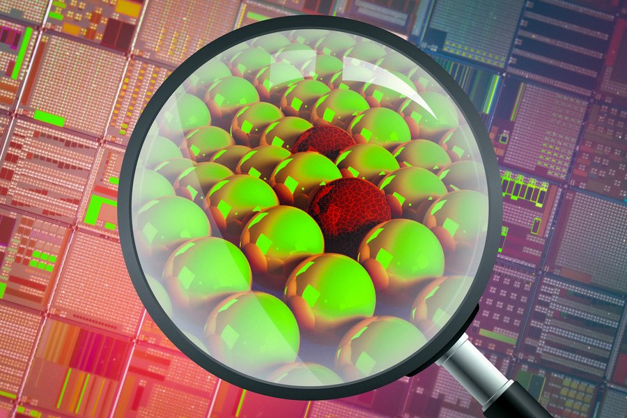
MIT researchers have developed an AI model that can detect and quantify up to six different atomic defects in materials simultaneously using non-destructive neutron scattering data, potentially revolutionizing quality control in semiconductor manufacturing and other industries.
MIT researchers have developed an AI model that can detect and quantify atomic-scale defects in materials without damaging them, potentially transforming how manufacturers ensure product quality and performance.
The breakthrough addresses a longstanding challenge in materials science: while engineers have become adept at intentionally introducing defects to enhance properties like strength and conductivity, measuring these defects accurately in finished products has remained difficult and often destructive.
The Hidden World of Atomic Defects
In materials science, defects aren't necessarily flaws—they're often carefully engineered features. Manufacturers deliberately introduce atomic-scale imperfections during production of semiconductors, steel, solar cells, and batteries to optimize performance. These defects can control electrical conductivity, improve mechanical strength, and enhance energy conversion efficiency.
However, understanding exactly what defects exist in a material and in what concentrations has been a guessing game. Traditional measurement techniques each capture only partial information, like the parable of blind men describing different parts of an elephant. Some methods can identify defect types but not concentrations, while others require destructive sampling.
AI Sees What Humans Cannot
The MIT team, led by associate professor Mingda Li and PhD candidate Mouyang Cheng, trained a machine learning model on 2,000 semiconductor materials using neutron-scattering data that measures atomic vibrations. The model employs a multihead attention mechanism similar to ChatGPT, learning to distinguish subtle differences in vibrational patterns between materials with and without defects.
"Existing techniques can't accurately characterize defects in a universal and quantitative way without destroying the material," Cheng explains. "For conventional techniques without machine learning, detecting six different defects is unthinkable. It's something you can't do any other way."
The model can identify up to six different point defects simultaneously, with concentrations as low as 0.2 percent. This represents a quantum leap from current capabilities, where manufacturers typically estimate defect quantities through slow, invasive testing of small sample batches.
From Theory to Practice
To validate their approach, the researchers tested the model on an alloy commonly used in electronics and a superconductor material. They successfully measured defect concentrations and even challenged the model with materials containing multiple defect types simultaneously.
"We were really surprised it worked that well," Cheng says. "It's very challenging to decode the mixed signals from two different types of defects—let alone six."
The technique uses neutron scattering to measure vibrational frequencies of atoms in solid materials. While powerful, this method requires specialized equipment that may not be readily available to all manufacturers. The researchers are now working to adapt their approach to Raman spectroscopy, a more widely used technique that measures light scattering.
Industry Implications
For semiconductor manufacturers and other industries that rely on precise material properties, this technology could enable real-time quality control without destroying products. Instead of testing a small percentage of items through invasive methods, companies could potentially scan every product on the production line.
The ability to detect unwanted defects—such as oxidation that occurs during manufacturing—could also prevent costly failures and improve yield rates. Engineers could verify whether their intentional defect engineering achieved the desired results without uncertainty.
A New Paradigm in Defect Science
Li describes the work as opening "a new paradigm in defect science." The AI approach can recognize patterns in defect signals that would appear identical to human observers, extracting meaningful information from what looks like noise.
"To the human eye, these defect signals would look essentially the same," Li notes. "But the pattern recognition of AI is good enough to discern different signals and get to the ground truth."
The research team, which includes collaborators from Oak Ridge National Laboratory, published their findings in the journal Matter. The work was supported by the Department of Energy and the National Science Foundation.
Future plans include expanding the model to detect larger features like grains and dislocations, and developing versions that work with more accessible measurement techniques. As Li puts it, "This opens up a new paradigm in defect science"—one where the hidden world of atomic imperfections becomes visible, quantifiable, and controllable without sacrificing the materials being studied.
For more information, visit the MIT News article or read the paper in Matter.
Comments
Please log in or register to join the discussion