Intel has quietly launched production at its Arizona-based Fab52, marking a pivotal moment in its quest to reclaim semiconductor leadership. The facility leverages breakthrough technologies like RibbonFET gate-all-around transistors and PowerVIA backside power delivery to outperform rivals. This 18A process node represents both a technical milestone for Intel's own chips and a critical test for its fledgling foundry business.
The Concrete Colossus: Intel’s Fab52 Goes Live
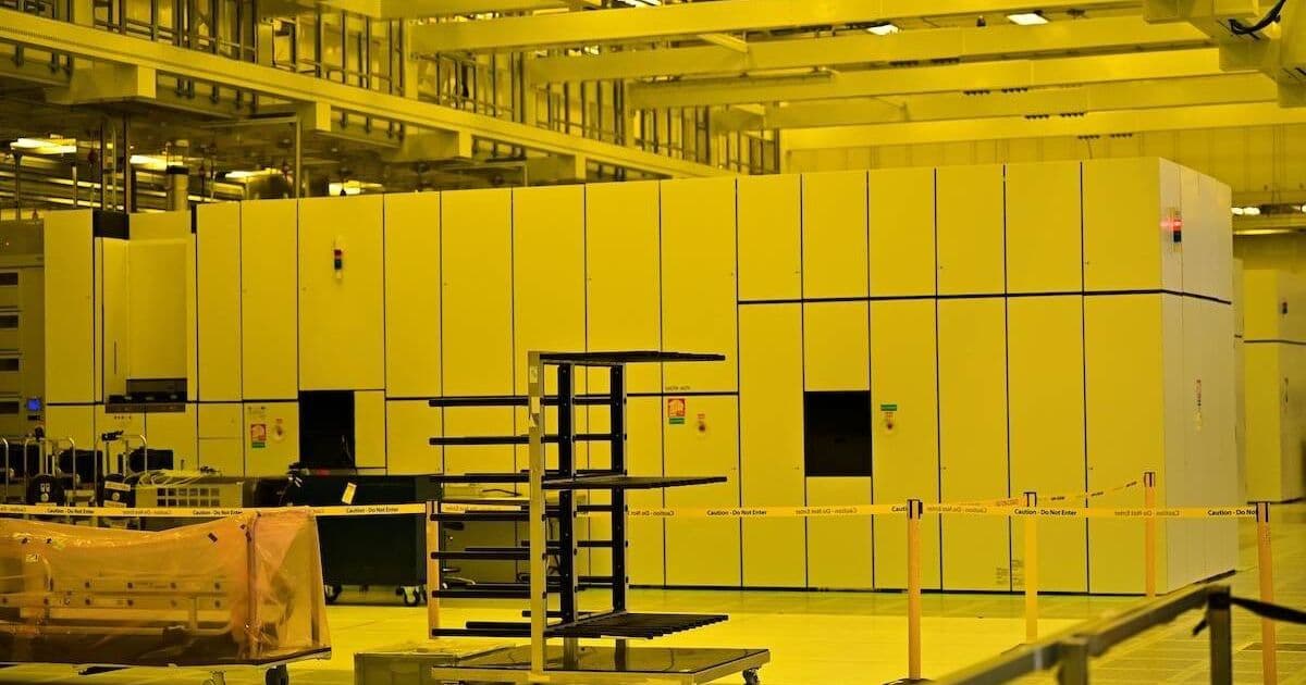
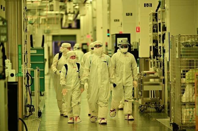
Four years after former CEO Pat Gelsinger unveiled Intel’s audacious plan to transform into a leading-edge foundry, its $20 billion bet is materializing within the sprawling, sterile halls of Fab52 in Chandler, Arizona. Covering one million square feet and built with 600,000 cubic meters of concrete and 110 tons of steel, Fab52 is now operational, mass-producing chips using Intel’s advanced 18A process node—a linchpin in the company’s comeback strategy. Access demands rigorous contamination control: workers don full-body "bunny suits" to maintain an environment with fewer than 10 particles per cubic foot of air, orders of magnitude cleaner than a hospital operating room.
Beyond EUV: The Anatomy of 18A Innovation
Stepping past the amber-lit lithography zones of the older Fab42 (where blue light sensitivity once reigned), Fab52 hums with the monolithic scale of ASML’s Extreme Ultra Violet (EUV) machines—each the size of a city bus. These tools vaporize tin droplets to generate plasma, etching infinitesimal circuits onto silicon wafers. But the real magic lies in 18A’s architectural leaps:
- RibbonFET (Gate-All-Around Transistors): Intel’s first production implementation of this design encases transistor channels entirely within the gate structure, slashing power leakage and boosting performance-per-watt by 15% over Intel 3. While Samsung debuted GAA earlier, Intel claims superior implementation maturity.

- PowerVIA (Backside Power Delivery): This industry-first move shifts power routing beneath the silicon wafer, freeing the top layers for signal routing. The result? A claimed 30% increase in transistor density and significantly cleaner power delivery—a feature TSMC won’t match until its A16 node arrives in late 2026.
"18A combines two transformative technologies ahead of anyone else: Gate-All-Around for efficiency and Backside Power for density. If yields hold, it’s a genuine technical leadership moment," observed one semiconductor analyst during the tour.
The Foundry Gambit: Panther Lake, Clearwater Forest, and the Search for Customers
Intel’s first 18A products—Panther Lake client CPUs (early 2026) and Clearwater Forest Xeons (late 2026)—serve a dual purpose. Technically, they aim to reclaim performance leadership: Panther Lake targets 10% better single-threaded perf/watt than its TSMC-made predecessors, while Clearwater Forest promises 17% more speed at 10% less power than Sierra Forest. Strategically, they are high-profile demos for Intel Foundry Services (IFS).
Yet, the foundry business faces headwinds. Despite 18A’s prowess, CEO Lip Bu Tan has bluntly stated that the future of IFS hinges on securing major external customers for the next generation, 14A (arriving 2027). The recent US government designation of Intel Foundry as a "national security asset" and $10 billion subsidy provides crucial backing, but commercial adoption remains the ultimate test. Intel is already refining 18A into variants like 18A-P (8% better perf/watt) and 18A-PT (optimized for 3D stacking), hoping to lure designers needing cutting-edge performance or advanced packaging.
The Weight of the Wafer
Fab52 stands as a monument to engineering ambition and Gelsinger’s initial vision. With 18A, Intel has demonstrably closed the process technology gap and even seized a temporary lead with PowerVIA. But the facility’s true success won’t be measured in wafers produced for Intel’s own CPUs alone. It will be judged by whether Tan can convince the industry’s skeptics—and potential customers—that Intel Foundry is a viable, competitive alternative to TSMC. The silicon is ready; the market’s verdict is pending.
Source: Tobias Mann, The Register (https://www.theregister.com/2025/10/12/gelsingers_foundry_dream_lives_on/)
Comments
Please log in or register to join the discussion