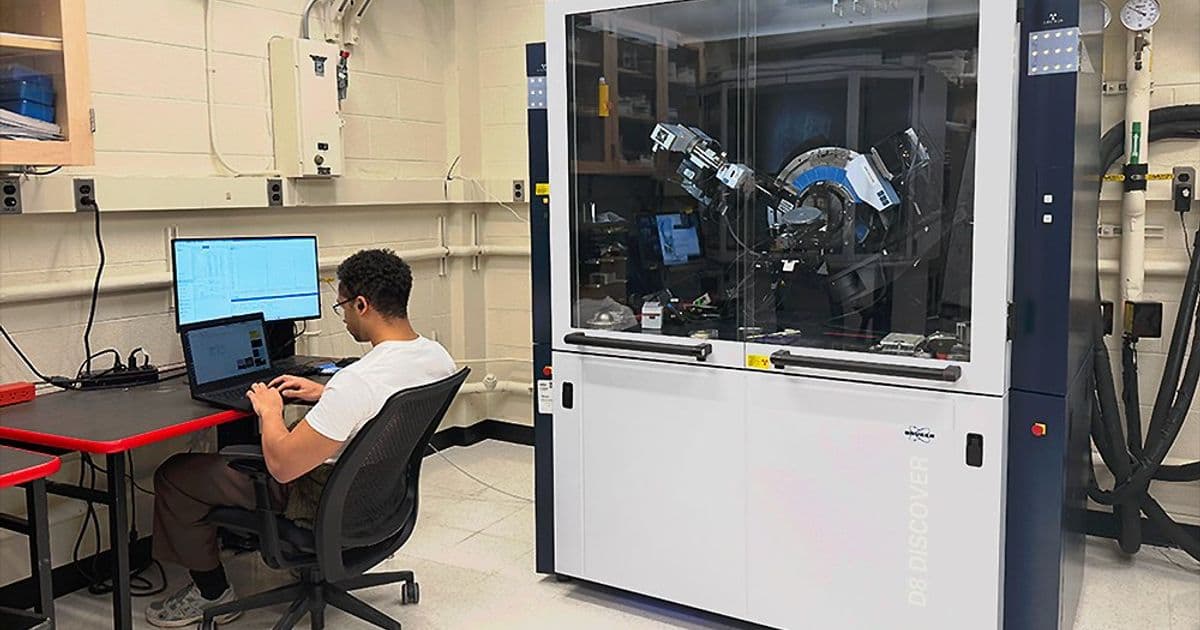
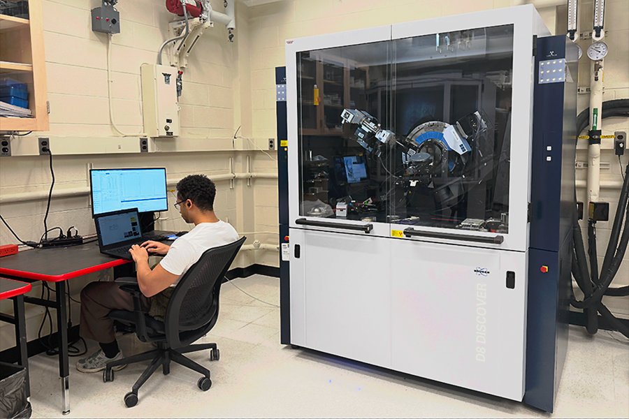
MIT.nano has installed the Bruker D8 Discover Plus, a high-resolution X-ray diffraction system that enables researchers to analyze materials at the nanoscale with unprecedented precision, supporting advances in electronics, energy storage, and nanotechnology.
MIT.nano has installed a new X-ray diffraction (XRD) instrument that significantly expands the institute's capabilities for analyzing materials at the atomic scale. The Bruker D8 Discover Plus, now operational within the Characterization.nano facility, represents a major upgrade to MIT's materials characterization toolkit, offering researchers unprecedented precision in examining crystalline structures, thin films, and nanoscale features.

Unlike conventional XRD systems scattered across MIT's campus, this new instrument features a high-brilliance micro-focus copper X-ray source that can target areas as small as 200 microns. This capability is particularly valuable for studying thin film samples where researchers need to analyze specific regions without interference from surrounding material. The system's large area detector captures comprehensive diffraction patterns, enabling detailed structural analysis of materials ranging from bulk metals to nanoscale coatings.
The technology builds on fundamental principles of X-ray diffraction, where X-rays interact with atomic planes in crystalline materials to produce interference patterns. These patterns reveal critical information about a material's crystalline phase, grain size, orientation, and defects. While many associate X-rays with medical imaging, XRD applies similar physics to probe the internal structure of materials without causing damage—a crucial advantage for studying delicate samples or monitoring changes over time.
For researchers across MIT, this capability translates into practical benefits. Civil engineers can analyze concrete mixtures to understand how different components affect long-term durability. Materials scientists can engineer new microstructures by tracking how atomic arrangements shift with varying element combinations. Electrical engineers studying semiconductor manufacturing can examine crystalline thin film deposition on substrates with unprecedented clarity.
The instrument's arrival addresses a critical bottleneck in materials research. "The addition of another high-resolution XRD will make it a lot easier to get time on these very popular tools," notes Fred Tutt, a PhD student in the Department of Materials Science and Engineering. The Bruker system's versatility also enables measurements that were previously difficult or impossible with existing equipment, supporting more experimental approaches and accelerating research timelines.
One of the most significant upgrades is the system's in-plane XRD capability, which allows researchers to study surface diffraction of thin films with non-uniform grain orientations. This technique proves particularly valuable for projects that begin in MIT.nano's cleanroom facilities. After depositing thin film coatings, researchers can selectively measure the top 100 nanometers of the surface, providing insights into surface quality and structural properties that affect device performance.
The Bruker D8 Discover Plus replaces two older systems, consolidating capabilities while adding new features. The microfocus source offers flexibility in spot size, ranging from 2mm down to 200 microns, allowing researchers to balance between flux intensity and spatial resolution depending on their specific needs. This adaptability proves essential when studying heterogeneous materials or when precise localization of measurements is required.
Beyond hardware capabilities, the system includes a comprehensive software suite for advanced data analysis. Research specialists Jordan Cox and Charlie Settens are currently training users not only in operating the diffractometer but also in interpreting the complex structural data it generates. This training ensures that researchers can extract maximum value from their measurements, moving beyond simple pattern collection to meaningful structural insights.
The timing of this installation aligns with growing demand for nanoscale characterization across multiple disciplines. As materials science increasingly focuses on engineered nanostructures and thin film technologies, tools capable of resolving atomic-scale features become essential. The Bruker system positions MIT.nano to support cutting-edge research in areas such as quantum materials, advanced energy storage systems, and next-generation electronics.
This addition follows a pattern of strategic investments in MIT.nano's characterization capabilities. The facility has recently expanded its portfolio with instruments supporting nanofabrication, plasma etching, and 3D nanoprinting. Each new tool addresses specific gaps in the research ecosystem, enabling more comprehensive materials studies from initial fabrication through final characterization.
The impact extends beyond individual research projects. By providing shared access to state-of-the-art characterization equipment, MIT.nano fosters collaboration across departments and disciplines. A material developed for energy applications might find unexpected uses in biomedical devices, with XRD analysis revealing properties that enable such cross-pollination of ideas.
For the broader scientific community, MIT.nano's investment signals the growing importance of nanoscale characterization in addressing global challenges. From developing more efficient solar cells to creating advanced medical diagnostics, understanding materials at the atomic level proves increasingly crucial. The Bruker D8 Discover Plus represents not just an incremental improvement but a qualitative leap in what's possible for materials analysis at MIT.
Researchers interested in utilizing the new system can access training and scheduling information through the Characterization.nano website. As the facility continues to expand its capabilities, it reinforces MIT's position at the forefront of nanoscale research and development, providing the tools necessary to tackle tomorrow's most pressing technological challenges.
Comments
Please log in or register to join the discussion