TSMC has detailed its comprehensive semiconductor manufacturing roadmap through 2029, introducing A12 and A13 processes for client devices, extending the N2 family with N2U, and confirming A16's 2027 launch. The company has adopted a bifurcated strategy, delivering annual client nodes and biennial HPC/AI nodes with distinct design priorities.
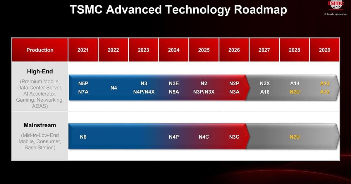
TSMC has revealed its ambitious process technology roadmap through 2029, showcasing a strategic bifurcation in node development that reflects the diverging requirements of the semiconductor market. At its North American Technology Symposium 2026, the company announced several new process technologies, including the 1.2nm and 1.3nm-class A12 and A13 processes, an unexpected N2U extension of its 2nm family, and confirmed the delayed launch of its premium A16 process to 2027.
The roadmap represents a significant shift in TSMC's approach to process technology development, moving away from a one-size-fits-all strategy toward a segmented approach that addresses the distinct needs of different market segments. "Last year we announced A14 as our most advanced, 2nd Generation nanosheet technology, scheduled for production in 2028," said Kevin Zhang, senior vice president of business development and global sales and deputy COO at TSMC. "This year, we are introducing derivatives of A14, including A13 and A12, both planned for production in 2029."
Dual-Track Process Strategy
Historically, TSMC's revenue was dominated by the smartphone industry, but AI and HPC applications have now outpaced handsets in importance. This market shift is reflected in the company's new strategy, which segments leading-edge nodes by end-market requirements rather than pursuing a uniform approach across all applications.
TSMC's roadmap now features two distinct tracks:
- Client applications (smartphones, client devices): New node introduced annually
- AI and HPC applications: New node introduced biennially
This differentiation acknowledges that client devices prioritize cost, power efficiency, and IP reuse, with strong design compatibility being highly valuable. In contrast, AI and HPC applications demand maximum performance improvements to justify technology transitions, with cost being a secondary consideration.
Client-Focused Nodes: Incremental Improvements with Compatibility
For client applications, TSMC is focusing on delivering incremental improvements while maintaining design compatibility. This approach enables customers to reuse existing intellectual property with minimal redesign effort.
A13: Optical Shrink of A14
The A13 process represents an optical shrink of the upcoming A14 process, designed to extract additional efficiency with minimal disruption. According to TSMC:
- Reduces linear dimensions by approximately 3% (to ~97% scale)
- Translates to roughly 6% higher transistor density
- Maintains full design-rule and electrical compatibility with A14
- Expected to enter production in 2029
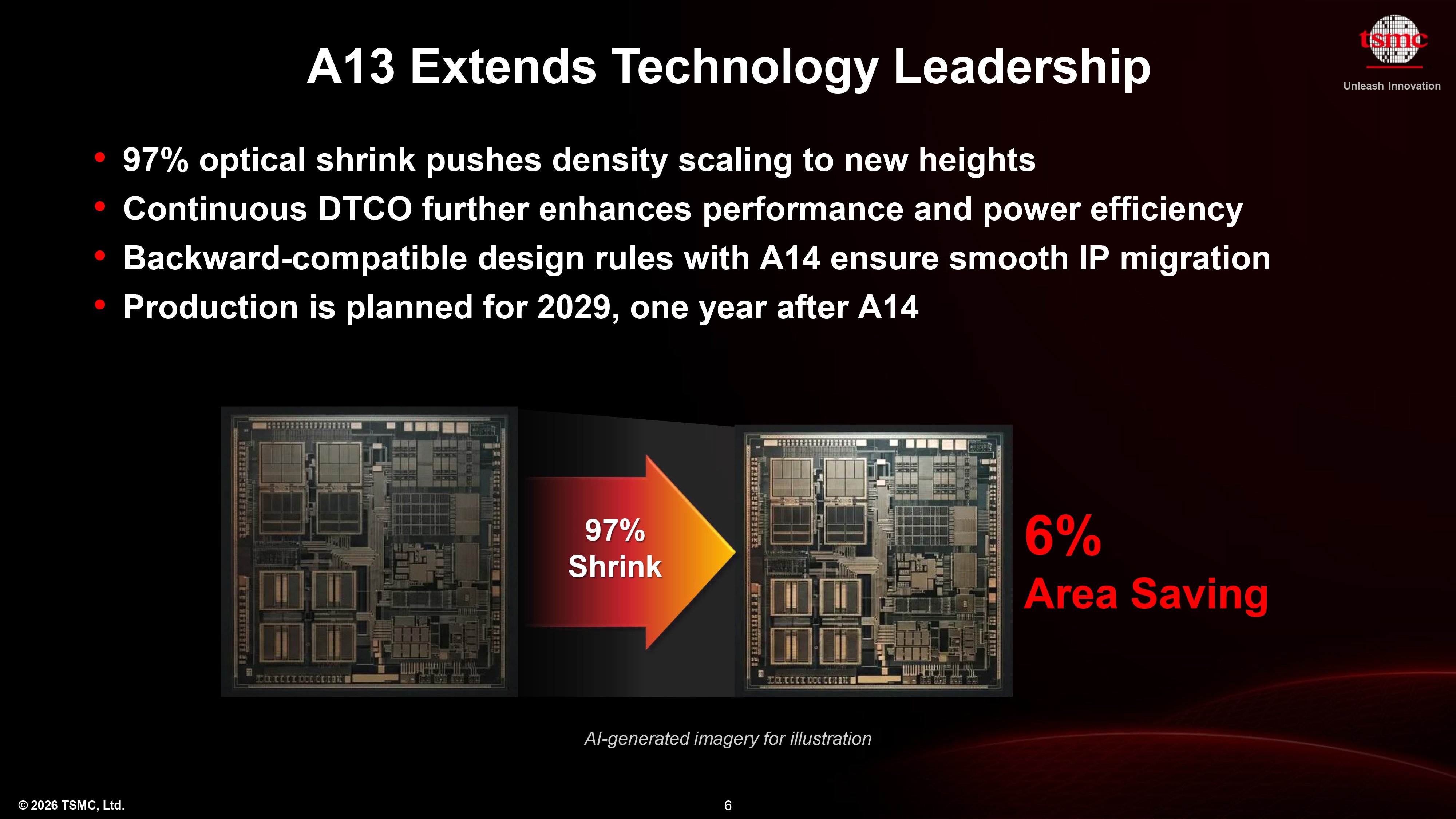
While A14 will deliver full-node improvements in power, performance, and density, requiring all-new design tools and methodologies, A13 achieves incremental gains through design-technology co-optimization (DTCO) without requiring changes to existing designs. This approach continues TSMC's tradition of offering optical shrinks of its process technologies, though the benefits are becoming more incremental as process scaling becomes increasingly challenging.
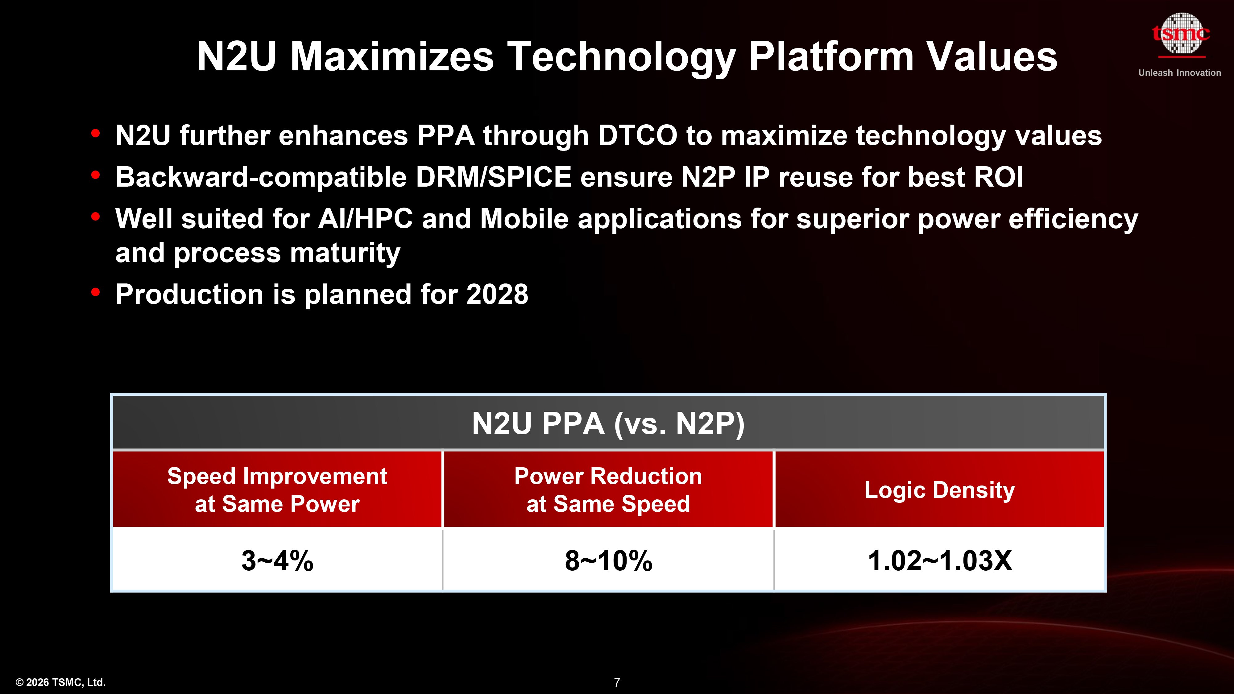
N2U: Extending the N2 Platform
In addition to A13, TSMC is introducing N2U, a third-year extension of the N2 platform that leverages DTCO to provide:
- 3-4% higher performance at the same power
- 8-10% lower power at the same speed
- 2-3% logic density improvement
Crucially, N2U maintains compatibility with N2P IP, enabling customers to build new products without transitioning to an entirely new process and incurring substantial costs. This compatibility is particularly valuable for companies developing mid-range products based on high-end IP implementations.
"We continue to extend our 2nm platform with N2U, which provides additional improvements in performance, power, and density through design-technology co-optimization," Zhang explained. "Our strategy is to continue enhancing each node after introduction, allowing customers to maximize the return on their design investments while still gaining incremental PPA benefits."
High-Performance Nodes: Maximum Performance at Any Cost
For AI and HPC applications, TSMC is developing a separate track of nodes that prioritize performance over cost and compatibility. These nodes integrate Super Power Rail (SPR) backside power delivery to address the power integrity and current delivery constraints of AI data center and HPC workloads.
A16: Delayed but Still Significant
TSMC has confirmed that the A16 process, originally planned for 2026, will now enter volume production in 2027. A16 represents N2P with SPR backside power delivery and will rely on 1st Generation nanosheet GAA transistors. While TSMC hasn't disclosed specific performance figures, A16 is expected to offer significant advantages over N2 and N2P nodes:
- Approximately 15-20% lower power consumption
- 8-10% performance improvement
- Higher transistor density
The delay doesn't indicate technical problems but rather reflects the production timeline. "A16 will be ready for production in 2026," Zhang clarified. "However, actual product ramp depends on customers, and we expect volume production to begin in 2027. That is why we aligned it to that timeline."
A12: The Next Generation of HPC Nodes
Following A16, TSMC will introduce A12 in 2029, which is projected to bring full-node advantages to the company's data center-class nodes. While specific details remain limited, A12 is expected to offer similar improvements over A16 as A14 brings over N2, featuring:
- 2nd Generation nanosheet GAA transistors
- NanoFlex Pro technology
- Enhanced backside power delivery capabilities
Interestingly, TSMC is also developing N2X, a performance-enhanced variant of N2P that uses traditional front-side power delivery to maximize clock speeds. This node will serve as a bridge between N2P and A16, providing a high-performance option for customers not yet ready to adopt the more complex SPR technology.
Lithography Strategy: Avoiding High-NA EUV
One of the most notable aspects of TSMC's roadmap is the company's approach to lithography. Unlike Intel, which plans to use High-NA EUV scanners for its 14A node and successors starting in 2027-2028, TSMC has confirmed that none of its nodes through 2029 will require High-NA EUV lithography.
"I tell you, I am amazed by our R&D team," Zhang remarked. "They continue to find a way to drive the technology scaling without using High-NA. One day they may have to use it, but at this point, we continue to be able to harvest the benefit from current EUV, not have to go to High-NA, which, you know, very, very expensive."
This approach allows TSMC to avoid the substantial capital expenditure associated with High-NA EUV tools, which cost approximately $150 million each and are significantly more complex to operate than current EUV scanners. By continuing to use conventional EUV technology, TSMC can maintain cost competitiveness while still delivering competitive process technologies.
Market Implications and Competitive Landscape
TSMC's bifurcated strategy reflects the increasingly diverse requirements of the semiconductor market. By developing separate tracks for client and HPC applications, the company can optimize each process for its target market's specific needs rather than compromising to serve all markets with a single process technology.
For clients, the annual cadence of new nodes provides a predictable upgrade path while maintaining design compatibility. For HPC and AI applications, the biennial cadence allows for more substantial architectural changes and the integration of complex technologies like SPR backside power delivery.
This strategy positions TSMC to compete effectively with both Samsung and Intel, which are pursuing different approaches to process technology development. Samsung has been aggressive with its GAA transistor implementation, while Intel has emphasized its aggressive cadence and use of High-NA EUV technology.
The roadmap also highlights TSMC's continued investment in R&D to extend Moore's Law through innovative techniques like DTCO and backside power delivery, rather than relying solely on traditional scaling approaches that are becoming increasingly expensive and difficult to implement.
As the semiconductor industry continues to evolve, TSMC's ability to balance technical innovation with practical manufacturing considerations will be critical to maintaining its leadership position in advanced process technology. The company's roadmap through 2029 demonstrates a clear understanding of market needs and a pragmatic approach to delivering value across different application segments.
Comments
Please log in or register to join the discussion