As AI accelerators grow larger and more complex, the industry is hitting fundamental constraints with 2.5D packaging. The solution isn't a single breakthrough but a fragmented ecosystem of trade-offs: thicker interposers that risk warpage, silicon bridges that struggle with assembly yield, and alternative materials like organic and glass substrates that remain years from viability.
The semiconductor industry has reached an inflection point where the most critical innovations aren't happening at the transistor level, but in how chips are packaged together. AI accelerators and high-performance computing devices have grown so large and bandwidth-hungry that traditional 2.5D integration approaches are straining under new economic and physical constraints that didn't exist five years ago.
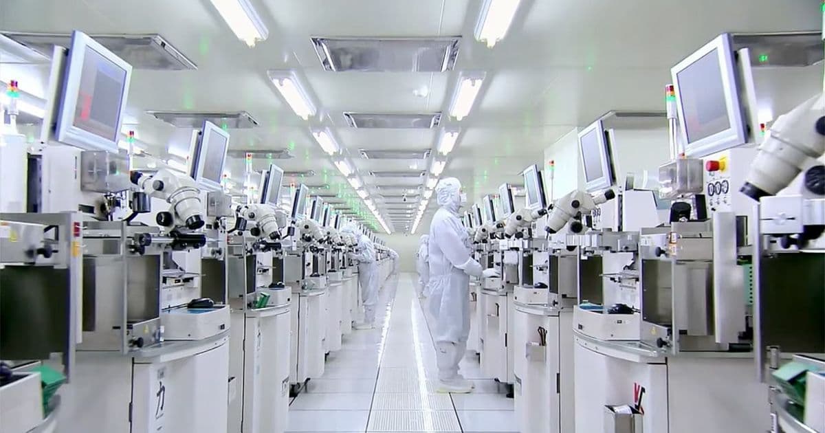
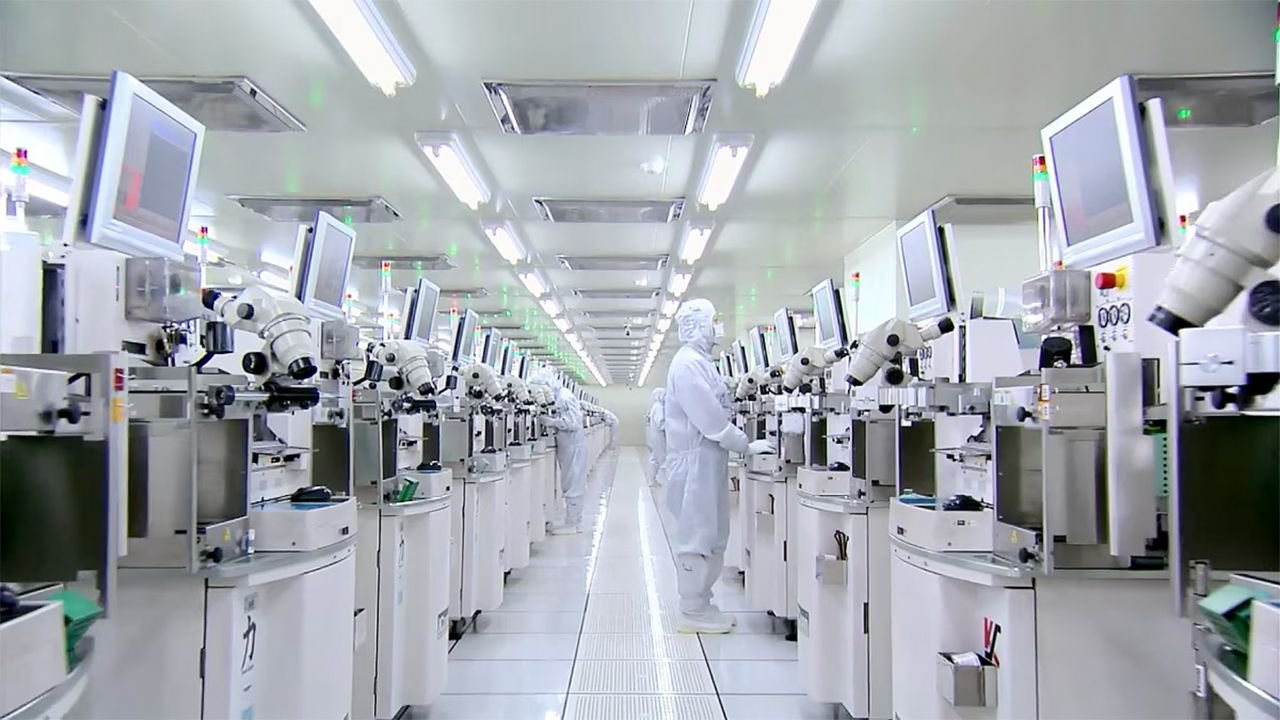
Packaging engineers across TSMC, Intel, Samsung, and ASE have quietly converged on a sobering reality: the interposer is no longer just a passive routing layer. It has evolved into a complex power delivery network, mechanical stabilizer, and signal integrity platform all at once. This transformation is forcing a fundamental rethinking of what 2.5D packaging means for cost, yield, and scalability in the AI era.
The Interposer Becomes a Power Platform
Early 2.5D packages used silicon interposers primarily as routing fabrics—thin silicon layers with through-silicon vias (TSVs) and fine-pitch metal routing to connect logic dies to adjacent memory stacks. The electrical requirements were modest, and four metal layers typically sufficed.
Today's AI accelerators tell a different story. High-Bandwidth Memory (HBM) interfaces have widened from 1024-bit to 2048-bit and beyond. Chiplet counts have multiplied. Power delivery requirements have intensified as compute dies push past 700W. The interposer must now handle substantial current while maintaining signal integrity across increasingly dense wiring.

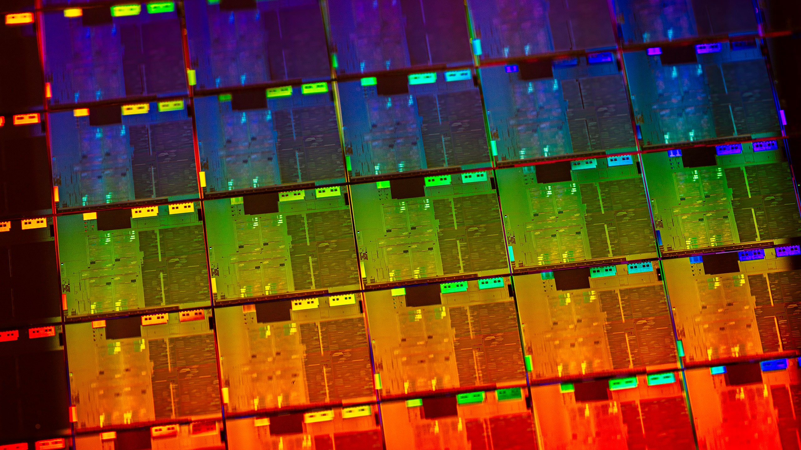
Vendors now routinely discuss interposers with eight, nine, or even sixteen metal layers. TSMC's roadmap for post-HBM3 systems explicitly targets these multi-layer architectures. Each additional metal layer increases fabrication cost by approximately 15-20%, but the mechanical implications are more problematic.
Thick, multilayer interposers are prone to warpage. Silicon's coefficient of thermal expansion (CTE) is 2.6 ppm/°C, while organic substrates range from 17-20 ppm/°C. This mismatch creates stress during thermal cycling, and controlling flatness across large interposers—now exceeding 800mm²—has become a critical assembly challenge.
Engineers are employing thin-film stress control techniques and tighter process windows to maintain flatness, but margins are narrowing. Thinner interposers reduce signal path lengths and improve electrical performance, but they're mechanically fragile. Thicker interposers offer stiffness and routing headroom, but increase thermal complexity and stress.
This trade-off has given rise to the active interposer concept. Once an interposer carries significant power infrastructure, the temptation to integrate logic becomes compelling. Active interposers can handle data movement, memory control, and even some preprocessing, reducing the burden on top-level compute dies.
However, active interposers fundamentally break the yield model. A passive interposer is a mechanical component—if it has a defect, it's scrap. An active interposer must be tested as a functional die, introducing new failure modes and validation steps. This means active interposers are largely confined to high-value AI and HPC designs where system-level benefits justify yield penalties.
Some vendors are already blurring these lines. Certain advanced packages use base dies that functionally resemble interposers but include active circuitry. These designs shift complexity downward, concentrating risk in fewer large silicon components while enabling more sophisticated system-level integration.
Silicon Bridges and the Yield Paradox
If interposers are becoming prohibitively expensive, silicon bridges were supposed to provide relief. The concept is elegant: replace a large, expensive silicon interposer with small, high-density bridge dies embedded directly in an organic substrate. Each bridge connects only adjacent chiplets, minimizing silicon area while preserving fine-pitch interconnect density.
Intel's Embedded Multi-die Interconnect Bridge (EMIB) and similar technologies exemplify this approach. The bridges themselves are small and yield well. The challenge is assembly: aligning multiple chiplets across those bridges with sufficient accuracy.
Placement offsets between dies are unavoidable at production scale. Typical pick-and-place equipment achieves ±5μm accuracy, but bridge-based interconnects require sub-micron alignment to maintain connectivity. These offsets can break finely patterned interconnects that rely on ideal alignment.
This creates a paradox. Bridges promise lower silicon cost, but misalignment during assembly can push overall package yields low enough that the solution becomes more expensive than a traditional silicon interposer. Some companies are experimenting with adaptive patterning techniques that compensate for placement offsets by modifying interconnect layouts after die placement. While this recovers yield, it introduces throughput penalties because patterning becomes die-specific.
Alternatively, relaxing design rules by using larger interconnect features can tolerate more misalignment, but this erodes the density advantage that justified bridges initially. There's a narrow operating window where bridges deliver both acceptable yield and meaningful cost savings.
Bridges continue to improve. Incremental gains in placement accuracy and adaptive processing may eventually unlock their potential, but they are not yet a universal substitute for silicon interposers.
Alternative Materials: Organic and Glass
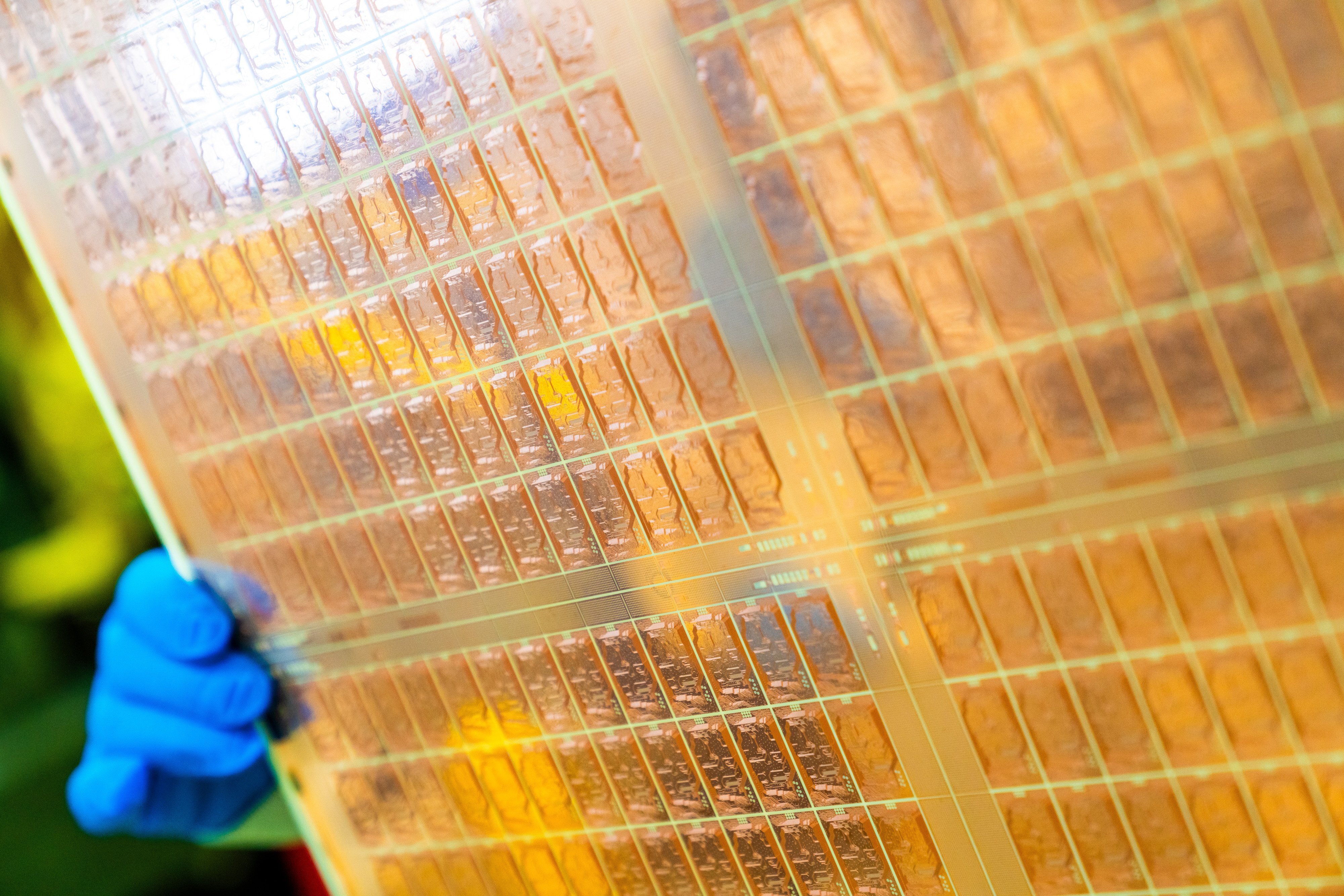
The longer-term effort to reduce 2.5D packaging cost focuses on alternative materials. Organic interposers are promising candidates because they can be built using panel-level processes, avoid expensive TSV formation, and scale naturally with existing substrate manufacturing infrastructure.

The challenge is density. Traditional package substrates operate at line/space dimensions of 15-20μm. Silicon interposers achieve 2-3μm. Pushing organic interposers down to five microns requires cleanroom environments and tighter process control, narrowing the cost gap with silicon. Advanced materials like Ajinomoto build-up films help, but they raise material costs even as they improve performance.
HBM integration complicates matters further. As memory interfaces tighten and stack counts increase, pad pitches shrink to 55μm and below. Silicon handles this comfortably, but organic materials struggle. Research efforts are underway to integrate HBM on organic interposers, but these remain experimental.
For the highest bandwidth designs, silicon remains the default because it offers predictable pitch control and proven reliability. Organic interposers are expected to coexist with silicon rather than replace it outright—viable where bandwidth and density demands allow, insufficient where they don't.
Glass interposers represent the next step beyond organic. They offer excellent electrical properties, low thermal expansion (approaching silicon), and compatibility with large panel formats. Glass also enables interesting possibilities for optical integration, since it's transparent and can host waveguides.
However, glass cannot host active circuitry, and the ecosystem required to process and standardize glass substrates at scale is still forming. With glass interposers, we're generally looking toward 2030 for volume production. Pilot lines have emerged, but widespread adoption depends on tooling maturity and supply chain development.
A Fragmented Path Forward
What's most apparent is that 2.5D packaging has fragmented into multiple parallel tracks, each addressing specific constraints but none offering a universal solution.
Silicon interposers are becoming thicker and more layered, pushing against mechanical and cost limits. Silicon bridges chase cost advantages but remain constrained by assembly yield. Organic and glass alternatives show promise but only within narrow application windows.
This fragmentation reflects a broader shift in semiconductor design. The industry is no longer optimizing purely for transistor density or clock speed. Instead, it's wrestling with system-level integration challenges where packaging, power delivery, mechanical stability, and economic viability are equally critical.
AI accelerators are the forcing function. Their insatiable demand for memory bandwidth and compute density has exposed weaknesses in packaging assumptions that worked for smaller, less complex devices. The solutions emerging—whether active interposers, adaptive bridge patterning, or alternative substrates—are incremental responses to fundamental physical and economic constraints.
The next five years will determine which approaches survive. For now, silicon remains the anchor, but its role is evolving from a simple routing layer to an active architectural component. The interposer isn't just part of the package anymore—it's part of the design.
Comments
Please log in or register to join the discussion