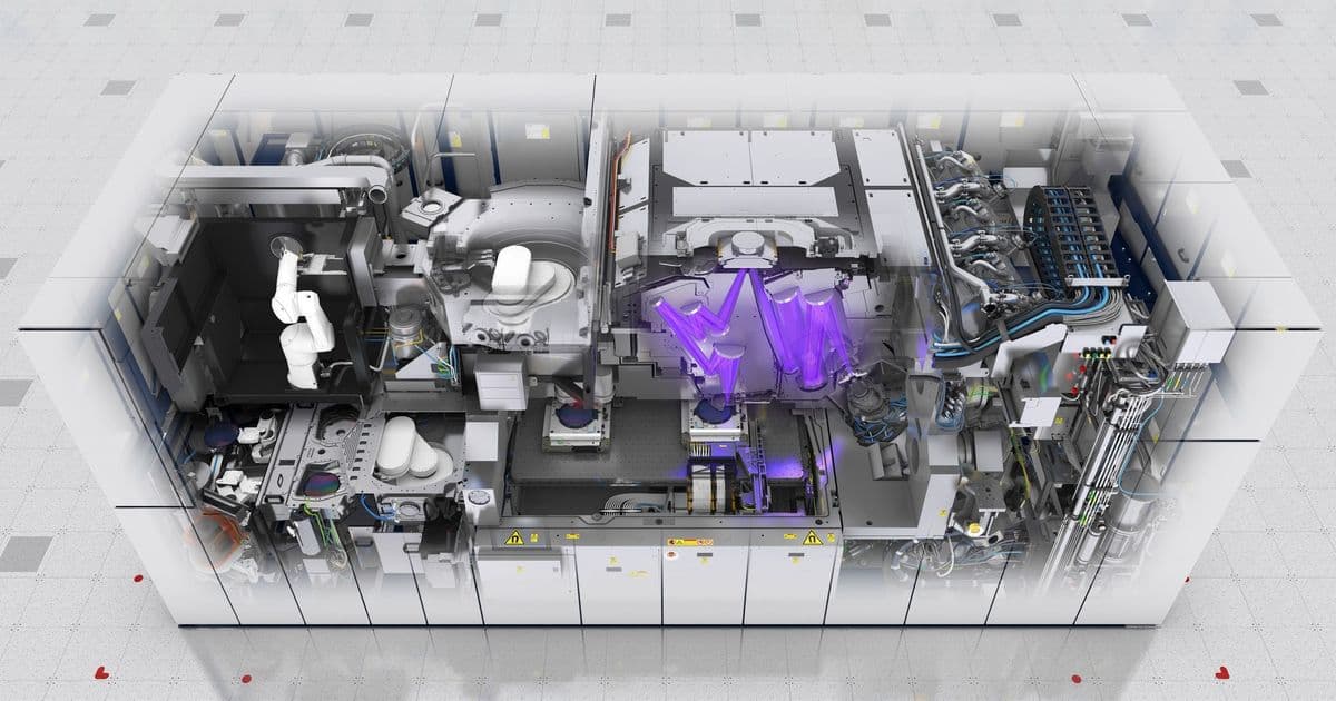
ASML has achieved a major milestone in EUV lithography with its 1,000W light source, using three precisely-timed laser pulses to generate extreme ultraviolet light from tin droplets at 100,000 per second. This breakthrough enables 50% higher productivity by 2030, but requires solving complex engineering challenges in debris management, optics, and wafer handling.
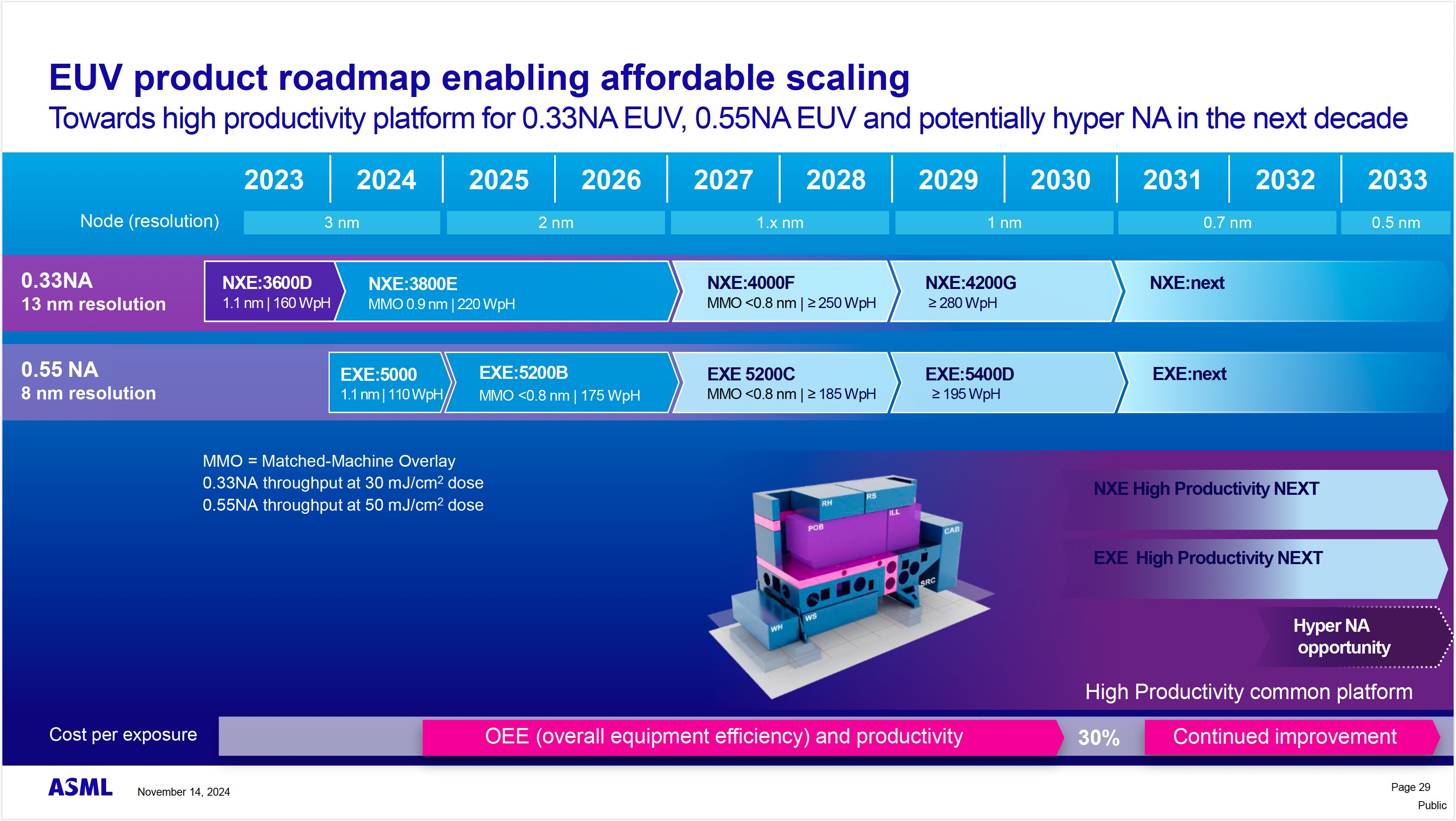
ASML has achieved a major breakthrough in extreme ultraviolet (EUV) lithography technology, announcing plans to deliver a 1,000-watt EUV light source by 2030 that will increase chipmaking productivity by 50%. The new Twinscan NXE system will process up to 330 wafers per hour, representing a significant leap from current-generation machines.
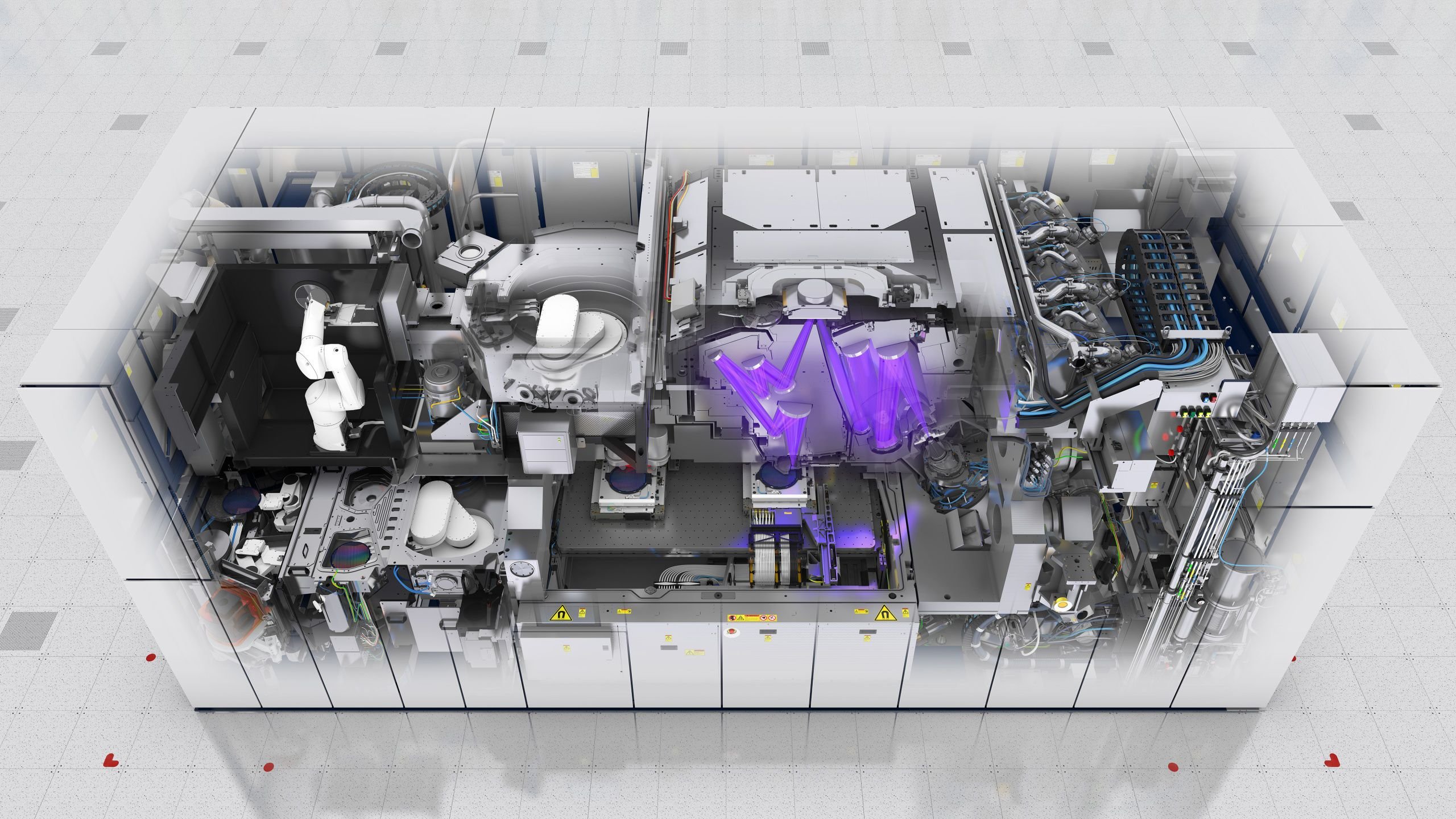
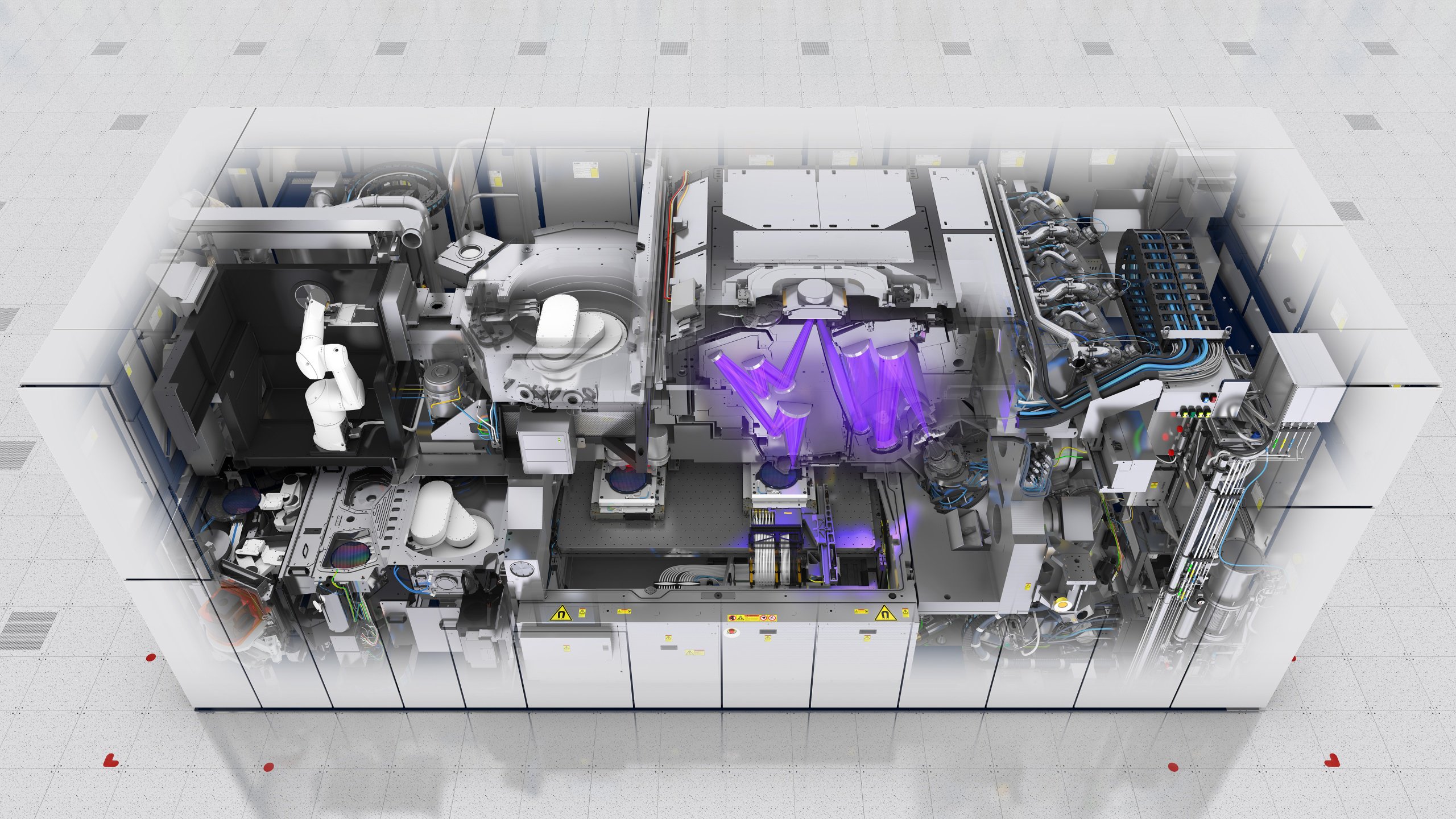
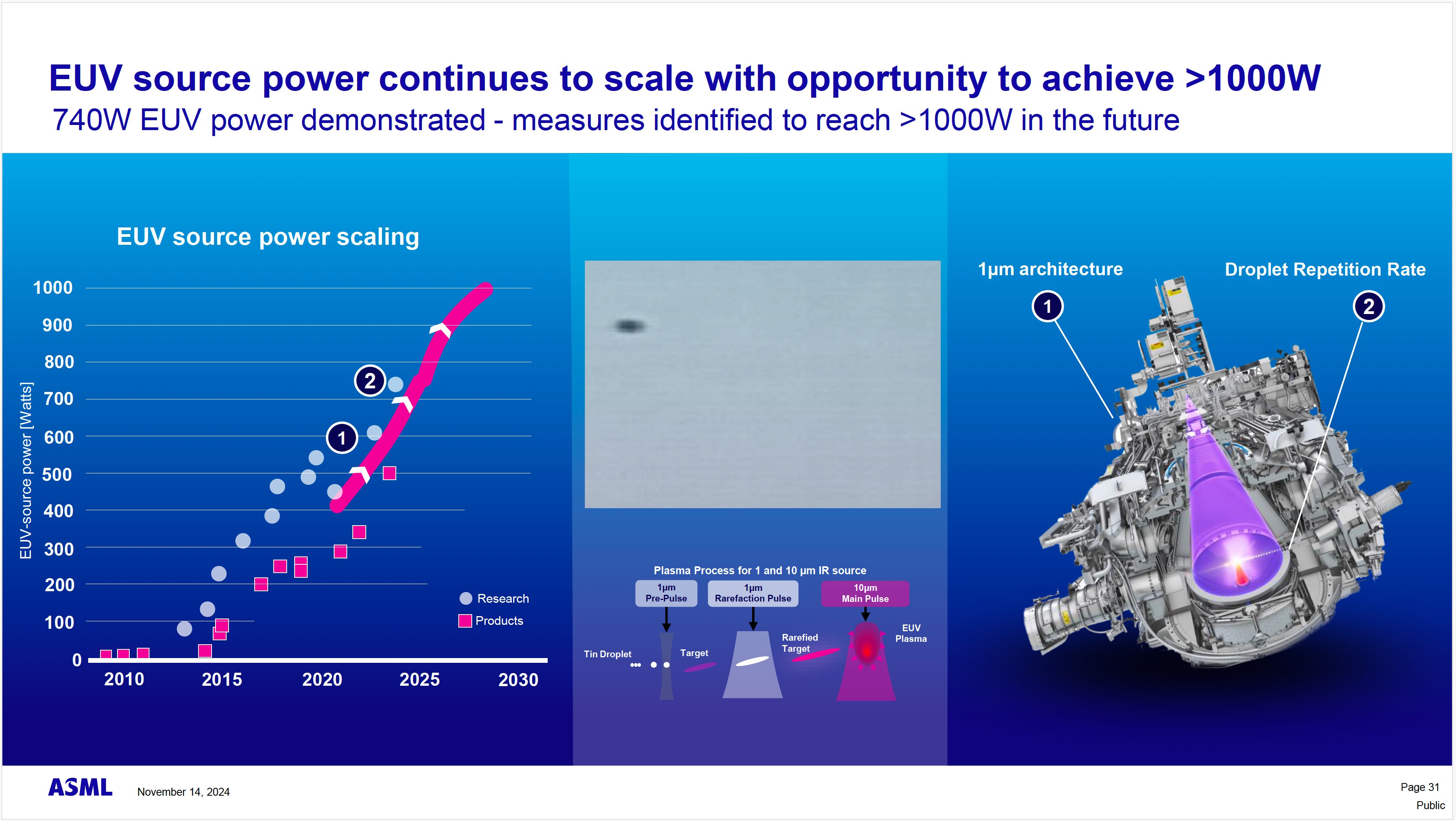
At the heart of this advancement lies a sophisticated three-pulse laser system that fires at 100,000 tin droplets every second. The process begins with a 1-micrometer pre-pulse that flattens each tin droplet, followed by a second 1-micrometer rarefaction pre-pulse that expands the droplet, and finally a 10-micrometer CO2 laser pulse that converts the prepared droplet into EUV plasma. This multi-stage approach represents a fundamental shift from previous single-pulse methods and enables the higher power output necessary for increased productivity.
The Physics of Power: From 250W to 1,000W
Current EUV systems like the NXE:3800E operate at around 250-300 watts of EUV power, processing approximately 220 wafers per hour. ASML's roadmap calls for scaling this to 1,000 watts by 2030, with the company's lead technologist Michael Purvis suggesting the technology could eventually reach 1,500 watts and potentially 2,000 watts.
The challenge isn't simply making the lasers more powerful. Each increase in power requires solving cascading engineering problems. More powerful lasers generate more heat, more debris, and place greater demands on every component in the system. The tin droplets themselves must be generated at twice the current rate—100,000 per second instead of 50,000—while maintaining precise uniformity.
Engineering the Impossible: System-Wide Innovation
Increasing EUV power output requires innovations across the entire lithography system:
Debris Management: Doubling the droplet rate means doubling the potential contamination. ASML must develop entirely new debris collection systems to prevent tin particles from reaching the reticle or wafer, which would cause defects.
High-Transmission Optics: Transferring 1,000 watts of EUV power to the wafer requires new projection optics with significantly higher transmission efficiency. These optics must maintain extreme precision while handling the increased energy load.
Wafer and Reticle Stages: Higher productivity demands faster, more precise positioning systems. The mechanical stages must move wafers and reticles with nanometer-level accuracy at increased speeds without introducing vibrations or positioning errors.
Resists and Pellicles: The photoresist materials and protective pellicles must be reformulated to work with the higher power levels and increased throughput, requiring collaboration across the entire semiconductor supply chain.
Timeline and Market Impact
The 1,000W system represents the culmination of ASML's long-term productivity roadmap. The company plans to introduce the Twinscan NXE:4000F in 2027 with over 250 wafers per hour capacity, followed by the NXE:4200G in 2029 with over 280 wafers per hour. The 1,000W system with 330 wafers per hour capability is targeted for 2030 or beyond.
This productivity increase translates directly to lower cost per wafer for chip manufacturers. A 50% increase in throughput means 50% more chips produced per hour, significantly reducing manufacturing costs for advanced nodes. This becomes particularly crucial as semiconductor manufacturers push toward 1.x-nanometer process nodes where the complexity and cost of each wafer are already extremely high.
The Competitive Landscape
ASML's announcement comes amid intense competition in the lithography equipment market. While ASML dominates the high-end EUV segment, competitors like Nikon and Canon continue developing DUV (deep ultraviolet) alternatives. China's semiconductor industry, facing export controls on EUV technology, is reportedly investing heavily in DUV capabilities and reverse-engineering efforts.
TSMC, one of ASML's largest customers, has announced $165 billion in U.S. investments, highlighting the strategic importance of advanced lithography technology. The ability to produce more chips per hour with higher yields directly impacts a foundry's competitiveness and profitability.
Technical Challenges Remain
Despite the breakthrough announcement, significant engineering challenges remain before the 1,000W system becomes commercially viable. The three-pulse laser system, while demonstrated in principle, must be integrated into a production-ready machine. The increased droplet generation rate requires new fluid dynamics control systems. The debris management solutions must prove reliable over millions of wafers.
ASML has yet to integrate this 1,000W capability into its Low-NA and High-NA EUV roadmaps, suggesting the technology may first appear in enhanced Twinscan NXE systems before migrating to next-generation High-NA platforms. The company's High-NA roadmap includes the EXE:5200C in 2025 and EXE:5400D in 2029, targeting the most advanced process nodes.
Looking Beyond 2030
Purves' mention of potential 1,500W and 2,000W systems suggests ASML views the 1,000W milestone as a stepping stone rather than a final destination. Each doubling of power output requires solving increasingly complex physics and engineering problems, but the economic incentives are substantial.
The semiconductor industry's insatiable demand for more transistors at lower cost continues to drive innovation in lithography technology. ASML's 1,000W breakthrough represents not just an incremental improvement but a fundamental advance in the physics of EUV light generation, potentially extending the viability of EUV lithography for several more technology nodes.
Comments
Please log in or register to join the discussion