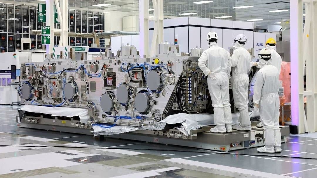
Imec used ASML’s new High‑NA EUV lithography to pattern 6 nm gate gaps for silicon spin‑qubit arrays, proving that the most advanced semiconductor manufacturing tool can meet the tolerances required for scalable quantum hardware. The move could align quantum‑chip production with the same roadmap that drives next‑gen AI processors, potentially shortening the path to fault‑tolerant quantum computers.
Imec Demonstrates First High‑NA EUV‑Fabricated Silicon Quantum Dot Qubit Device
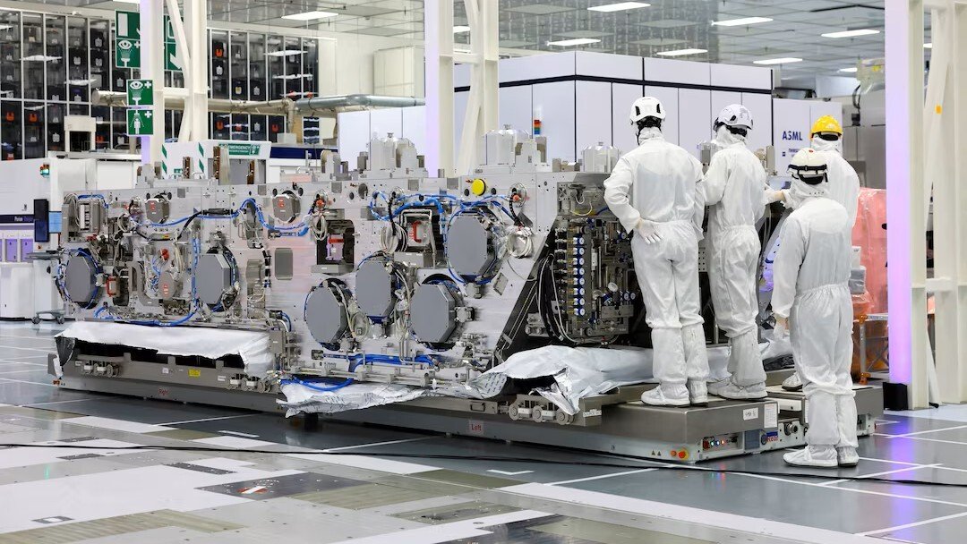 Image credit: Imec
Imec announced on 19 May at ITF World in Leuven that it has fabricated a silicon quantum‑dot spin‑qubit array using ASML’s High‑NA EUV lithography platform. The device features gate‑to‑gate spacings of just 6 nm, the smallest feature size ever printed for a quantum‑hardware structure on a 300 mm wafer.
Technical specifications
| Parameter | Value | Relevance |
|---|---|---|
| Lithography tool | ASML High‑NA EUV (NA 0.55) | Enables sub‑10 nm patterning at production‑grade overlay and CD control |
| Wafer size | 300 mm | Directly compatible with mainstream CMOS fabs |
| Gate gap (plunger‑to‑barrier) | 6 nm | Determines exchange coupling; tighter gaps increase two‑qubit gate speed exponentially |
| Qubit type | Silicon quantum‑dot spin | Leverages long electron‑spin coherence in isotopically purified ^28Si |
| Operating temperature | ~20 mK (dilution refrigerator) | Standard for spin‑qubit platforms |
| Measured single‑qubit fidelity* | 99.5 % | Comparable to leading superconducting qubits |
| Measured two‑qubit gate fidelity* | 98.8 % | Shows that 6 nm spacing yields strong exchange coupling |
*Values are from Imec’s internal test structures; full system metrics are still under development.
Why High‑NA EUV matters
Conventional EUV (NA 0.33) can reliably print features down to ~13 nm on 300 mm wafers. By increasing the numerical aperture to 0.55, the High‑NA system reduces the diffraction‑limited spot size by roughly 30 %, allowing critical dimensions (CD) of 6–8 nm with the same process window. The trade‑off is a larger, heavier optical column (≈150 t) and a reduced exposure field, which makes the tool expensive (>$200 M) and limited to high‑volume manufacturers.
For silicon spin qubits, the exchange interaction between neighboring electrons scales as (J \propto e^{-d/\lambda}), where (d) is the inter‑dot spacing and (\lambda) is a material‑dependent decay length (~1 nm). Reducing (d) from 10 nm to 6 nm therefore boosts (J) by a factor of ~4‑5, translating directly into faster two‑qubit gates (sub‑100 ns) and higher fidelity. Achieving that spacing uniformly across a wafer has been the missing piece for moving from laboratory‑scale devices (often hand‑crafted with e‑beam) to a production‑ready process.
Market and supply‑chain implications
- Alignment with AI‑processor roadmaps – High‑NA EUV is being qualified for sub‑2 nm logic nodes that will power next‑generation AI accelerators. Imec’s use of the same tool for quantum devices means that once the lithography platform reaches volume production, quantum‑chip fabs could piggy‑back on the same mask‑making and wafer‑fab infrastructure.
- Cost amortization – A single High‑NA EUV tool spreads its capital expense over billions of logic chips per year. If quantum‑chip volumes reach even a few hundred thousand wafers annually, the per‑qubit cost could drop from the current $10⁴–$10⁵ range to a few hundred dollars, making cloud‑based quantum services economically viable.
- Supply‑chain convergence – Materials such as high‑purity ^28Si, low‑k dielectrics, and advanced metal gates are already sourced for leading‑edge CMOS. Quantum‑dot production can source from the same supply chain, avoiding the need for a separate ecosystem of specialty foundries.
- Timeline compression – Industry roadmaps for fault‑tolerant quantum computers (millions of logical qubits) currently project 2030‑2035 as the earliest horizon, largely because of manufacturing bottlenecks. If High‑NA EUV becomes the standard lithography for both AI chips and quantum dots, the scaling curve could shift left by 3–5 years, assuming yield improvements keep pace.
- Competitive positioning – Intel, TSMC, and Samsung have all announced pilot lines for High‑NA EUV. Imec’s early demonstration gives European quantum‑hardware programs a foothold in the same technology node, potentially attracting government and hyperscaler funding aimed at co‑developing AI and quantum silicon.
What remains to be done
- Yield and defectivity – Current test structures show functional qubits, but wafer‑scale defect maps are still being compiled. Even a 0.1 % defect rate could cripple a 1‑M‑qubit array.
- Integration of control electronics – Spin‑qubit control requires cryogenic CMOS drivers. Co‑fabricating these drivers on the same die (or on a 3‑D‑stack) will be the next manufacturing hurdle.
- Error‑correction overhead – Fault‑tolerant operation still demands >1 000 physical qubits per logical qubit. Scaling from a handful of test qubits to that regime will test the limits of High‑NA EUV’s overlay precision.
- Tool availability – With only a handful of High‑NA EUV machines installed worldwide, capacity constraints could become a bottleneck unless new units are commissioned.
Bottom line
Imec’s 6 nm quantum‑dot array proves that the most advanced lithography tool in the semiconductor industry can meet the dimensional tolerances required for silicon spin qubits. The breakthrough is less about a sudden leap in quantum performance and more about bringing quantum hardware onto the same manufacturing roadmap that underpins next‑generation AI processors. If the industry can solve the remaining yield and integration challenges, the convergence could shave years off the timeline to practical, fault‑tolerant quantum computers, while leveraging the massive economies of scale already built for CMOS.
Comments
Please log in or register to join the discussion