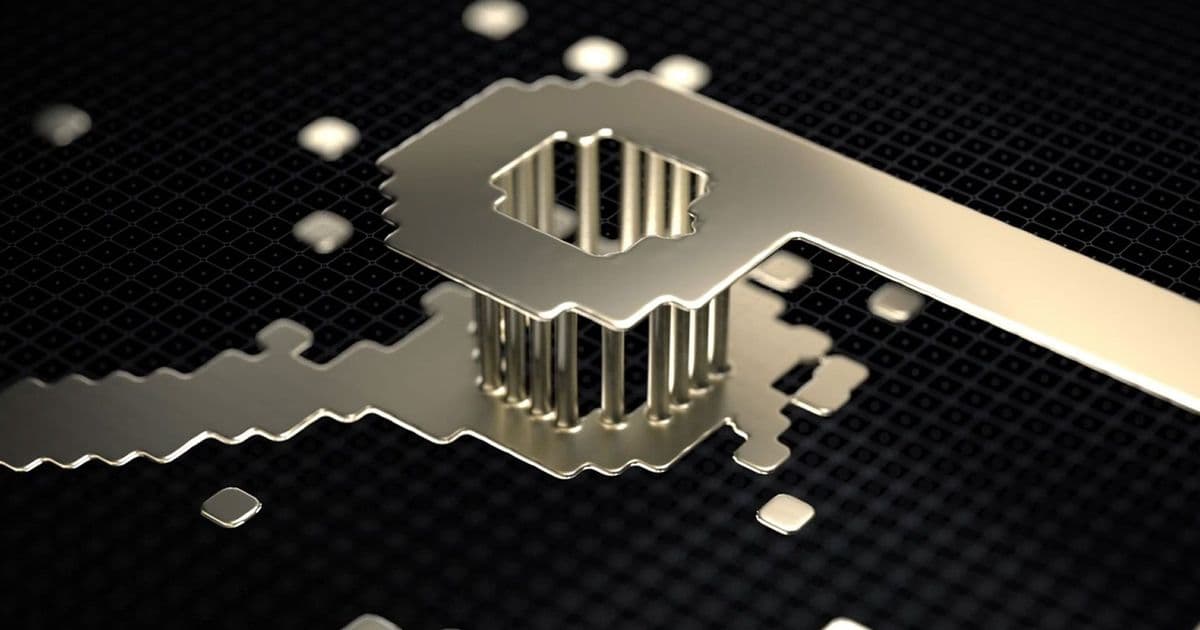
Itera has emerged from stealth with a prototype that uses electrowetting to move liquid‑metal traces on a glass substrate, allowing physical rewiring of a circuit in under a minute. The startup says the approach could compress hardware prototype cycles by three orders of magnitude, while its $12 M seed round and early OEM interest suggest a path to commercial deployment.
Announcement
Itera, a deep‑tech startup focused on reconfigurable hardware, announced a working prototype of what it calls the world’s first fluid circuit board. The device relies on electrowetting to shift liquid‑metal alloys across a glass substrate in response to electric fields, enabling engineers to re‑route a physical circuit in less than a minute. The company frames the breakthrough as a hardware analogue to the rapid edit‑compile‑run loop that software developers have enjoyed for decades.
Technical specifications
- Substrate: Borosilicate glass, 0.5 mm thick, offering a smooth, chemically inert surface for liquid‑metal flow.
- Conductive medium: Gallium‑indium‑tin (GaInSn) alloy, liquid at room temperature, with a resistivity of ~29 µΩ·cm, comparable to bulk copper.
- Actuation method: Electrowetting electrodes patterned beneath the glass create localized electric fields (typically 5–10 V, 1 kHz). Adjusting the field polarity changes the surface tension, pulling the alloy into the desired trace geometry.
- Resolution: Minimum trace width of 100 µm, line‑to‑line spacing of 150 µm, sufficient for most mixed‑signal boards up to 2 GHz signal‑path frequencies.
- Layer count: Current prototype supports a single active fluid layer with optional static copper planes for power distribution; future versions aim for 4‑layer stacks.
- Reconfiguration speed: Full board rewrite measured at 45 s on a 10 cm × 10 cm test panel, including fluid stabilization and component placement.
- Component integration: Standard surface‑mount devices (SMDs) are placed on the glass after the fluid pattern is set. The metal traces conform around the component leads, providing a true electrical connection rather than a simulation.
How electrowetting works in this context
Electrowetting modifies the contact angle of a liquid on a dielectric surface by applying a voltage across a thin insulating layer. In Itera’s board, the glass is coated with a nanometer‑scale hydrophobic dielectric, then overlaid with a patterned electrode grid. When a voltage is applied, the liquid‑metal alloy spreads into the energized cells, forming a conductive path. Reversing the voltage collapses the path, allowing the fluid to retreat to a neutral reservoir. This mechanism is analogous to how modern e‑ink displays move pigment particles, but with orders of magnitude higher conductivity.
Trade‑offs and challenges
| Aspect | Advantage | Limitation |
|---|---|---|
| Speed | Rewrites under 1 min vs. days for traditional fab | Fluid stabilization adds a few seconds; not instantaneous |
| Electrical performance | Resistivity close to copper; supports MHz‑range signals | Higher parasitic capacitance due to dielectric layers; not yet proven at multi‑GHz |
| Thermal handling | Liquid metal spreads heat, reducing hot‑spots | Gallium alloys solidify at ~10 °C; requires temperature control in cold environments |
| Manufacturability | No photolithography steps for each iteration | Requires precise electrode fabrication and clean‑room handling of liquid metal |
| Reliability | Reconfigurable; no permanent etch defects | Potential for alloy oxidation over many cycles; long‑term wear of dielectric unknown |
Market implications
Acceleration of hardware development cycles
If the claimed 1,000× speedup holds across typical design flows, a three‑week PCB prototype cycle could shrink to under three hours. That compression would align hardware development timelines with agile software sprints, allowing teams to test analog front‑ends, power‑management schemes, or RF matching networks in near‑real time. Companies that rely on rapid iteration—autonomous‑vehicle sensor stacks, edge‑AI ASICs, and defense prototyping—could see billions of dollars in saved NRE (non‑recurring engineering) costs.
Supply‑chain considerations
Itera plans to operate an Electronics‑as‑a‑Service (EaaS) model, where designs are uploaded to a secure U.S. testing center, components are placed, and the fluid substrate is reconfigured on demand. This model reduces the need for multiple physical mask sets and long‑lead‑time fab runs. However, it also introduces a new bottleneck: the capacity of the fluid‑reconfiguration facilities. Scaling to volume production will require parallelizing the electrowetting rigs and ensuring consistent alloy purity.
Competitive positioning
Traditional rapid‑prototype solutions—such as CNC‑milled FR‑4, 3‑D‑printed conductive filaments, or modular breadboard systems—still require manual wiring or post‑process soldering. Itera’s approach offers true electronic behavior (inductance, capacitance, and resistance) because real components are mounted on the fluid traces. Competitors like Molex’s 3‑D‑printed interconnects or Intel’s reconfigurable analog fabric focus on either low‑frequency prototyping or on‑chip reconfiguration, leaving a niche for a mid‑frequency, multi‑component fluid board.
Early adopters and funding
The startup secured $12 M in seed financing from Upfront Ventures, Costanoa Ventures, and Colle Capital. A top‑5 automotive OEM and a defense prime have already reserved the first production run, indicating confidence in the technology’s potential for high‑reliability, safety‑critical applications. Interest from a leading hyperscaler suggests that data‑center ASIC designers may eventually use fluid boards for early‑stage verification before committing to silicon.
Outlook
Itera’s fluid PCB represents a hardware‑centric shift toward software‑like iteration speeds. The key success factors will be:
- Demonstrating repeatable electrical performance across temperature and cycle‑count ranges.
- Scaling the electrowetting infrastructure to handle dozens of concurrent redesigns.
- Building a robust supply chain for ultra‑pure liquid‑metal alloys and dielectric coatings.
If these hurdles are cleared, the industry could see a new class of rapid‑prototype boards that bridge the gap between breadboard flexibility and production‑grade performance, fundamentally altering how engineers approach electronic system design.
For more details on electrowetting fundamentals, see the MIT research page.
Comments
Please log in or register to join the discussion