As the semiconductor industry approaches the physical limits of Moore's Law, TSMC, Intel and Samsung are pursuing divergent strategies in their quest for process leadership, with distinct approaches to node scaling, transistor architecture, and power delivery that will shape the chip landscape for the remainder of the decade.
The amount of capital, expertise, and experience required to develop leading-edge process technologies and build high-volume fabs supporting advanced nodes is so substantial that only three companies in the world are currently capable of producing them. Companies like Rapidus have yet to prove they are viable leading-edge chipmakers in this exclusive club. 
As the industry approaches the physical limits of traditional scaling, all three leading foundries are transitioning from conventional node naming conventions to a more segmented, architecture- and product-driven approach. However, they are pursuing these strategies with different priorities and timelines, creating a complex competitive landscape that will shape the semiconductor industry for years to come.
TSMC: Execution Excellence and Market Segmentation
TSMC maintains its position as the world's largest contract chipmaker with the most structured and execution-focused roadmap among the three foundries. The company initiated mass production of chips using its N2 process technology — its first node with GAA nanosheet transistors — at two fabs simultaneously late last year. This dual-fab launch is unprecedented in the industry and reflects the structural changes caused by overwhelming demand from the AI segment.
TSMC's approach is characterized by predictable scaling combined with aggressive specialization, which is why its roadmap is split into two distinct paths: high-performance computing-oriented technologies with backside power delivery network (BSPDN) and cost/density-optimized nodes without it. This segmentation allows TSMC to address different market segments with appropriate technologies rather than forcing all customers onto the most expensive nodes.
The company is on track to start producing chips using performance-enhanced N2P with traditional frontside power delivery and A16 technology that adds backside power delivery on top. Looking ahead, TSMC will continue offering advanced technologies with and without BSPDN, as this feature may be too expensive for consumer and smartphone applications but clearly valuable for heavy-duty data center processors. For example, A14 will emerge as a smartphone-oriented node in 2028, but will re-emerge as a data center-oriented node once it gets BSPDN in 2029. 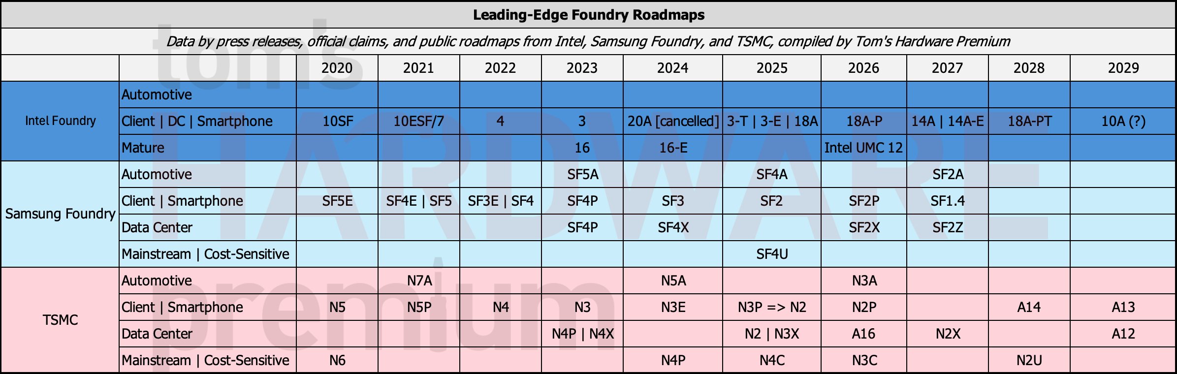
TSMC's segmentation strategy extends to its mainstream nodes like N4C, N3C, and eventually N2C for applications more sensitive to costs. Automotive-specific nodes (N7A, N5A, N3A) will lag leading-edge nodes by one to two generations, as they prioritize reliability and longevity over performance and transistor density.
This yearly cadence for advanced manufacturing nodes and wide range of options enable TSMC to address the most demanding clients like Apple, AMD, Intel, Nvidia, or Qualcomm with competitive process technologies. Ultimately, such discipline reinforces TSMC's position as the most predictable and commercially successful foundry in the industry.
Intel: The Aggressive Challenger
Intel's foundry division represents the most ambitious but arguably the most volatile roadmap when compared to its competitors. As a new player in the foundry market and a large integrated design manufacturer (IDM), Intel is pursuing a multi-faceted strategy aimed at addressing both its own product needs and attempting to capture customers that do not necessarily require leading-edge process technologies.
Intel's roadmap is built around aggressive technological milestones. With its 18A and subsequent process technologies, Intel bet on the simultaneous implementation of gate-all-around (GAA) RibbonFET transistors and a BSPDN to maximize performance, power efficiency, and transistor density. This dual implementation was a strategic decision to differentiate Intel from competitors who were introducing these technologies separately.
Looking ahead, Intel is targeting 14A and 14A-E for 2027-2028 production readiness. These nodes will introduce Intel's 2nd Generation RibbonFET GAA transistors, revamped PowerDirect backside power delivery, and Turbo Cells to improve the performance of critical data paths. Most significantly, these will be the company's first nodes to use High-NA EUV lithography, at least for some variants, which will be another attempt to introduce a technology that differentiates Intel compared to competing nodes.
Intel has indicated that interest in 14A from external customers is significant. Elon Musk's Terafab project is set to make use of Intel's 14A, as a licensee, but not as a customer. At the same time, Intel is heavily relying on node variants to address different use cases, including performance enhancements (P), feature enhancements (E), and through-silicon via support (T). These process technologies are required to enable Intel to build custom multi-chiplet products for consumer and data center applications, which directly support its strategy to produce most of its products at in-house fabs.
Beyond its leading-edge nodes, Intel's roadmap includes continued investment in mature nodes such as Intel 16 and UMC 12 as the company pursues a strategy to capture demand outside leading-edge applications, ensuring steady revenue streams while it develops its advanced technologies. 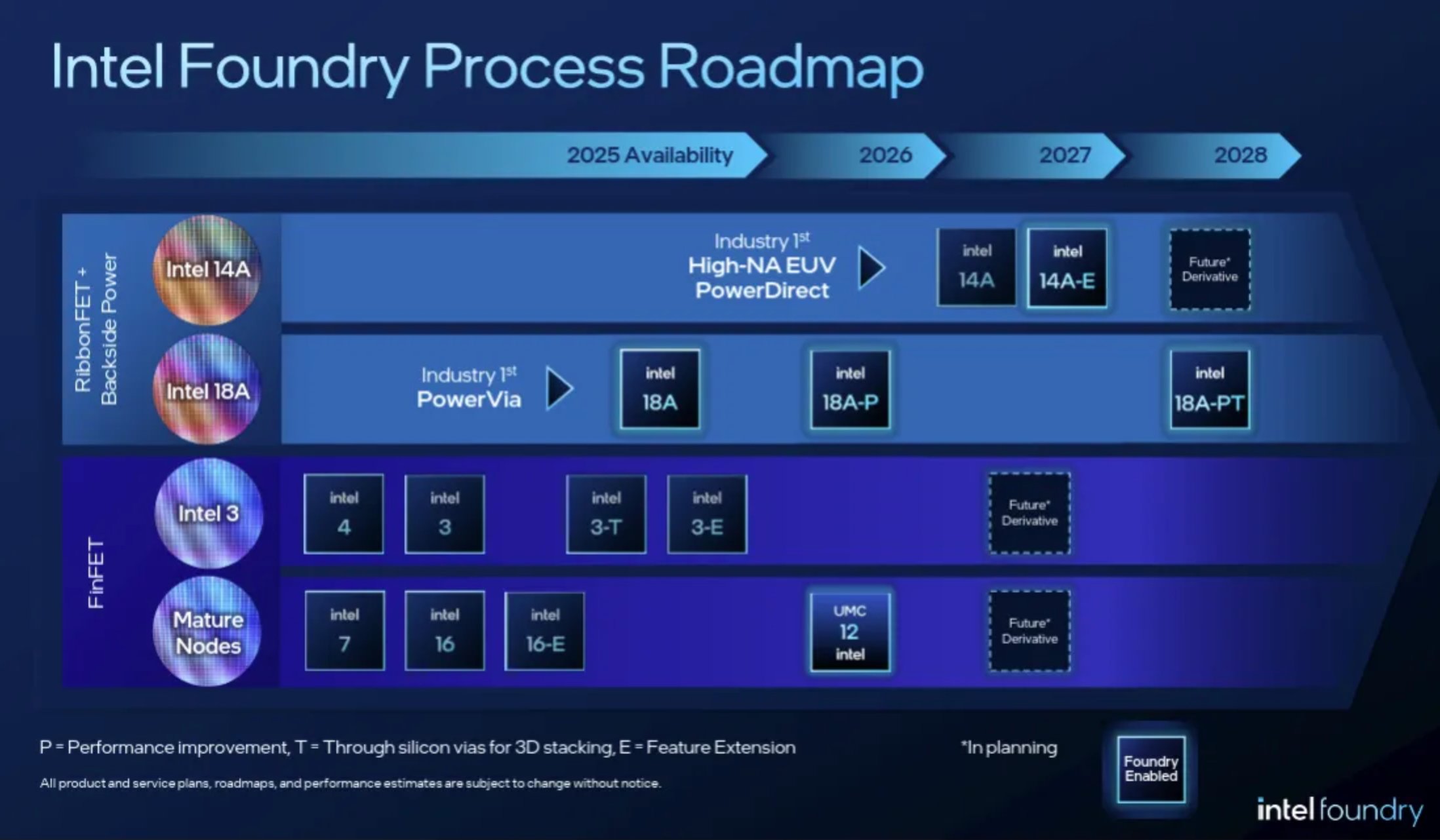
However, the abrupt cancellation of 20A in late 2024 highlights the execution risks associated with such an aggressive roadmap. This cancellation suggests Intel may be facing technical challenges that could affect its ability to maintain its ambitious timeline.
Samsung: Yield-Focused Evolution
Samsung was the first company to adopt GAA transistors with its SF3E technology in 2022, three years before Intel and TSMC. However, low and unpredictable yields have limited the adoption of this technology to niche applications like cryptocurrency mining ASICs. While SF3 was more mature, it was still adopted by select applications, mostly internally.
As a result, the highest-performing chips made by Samsung are currently produced using FinFET-based SF4P and SF4X, which puts the company behind its rivals in terms of process technology leadership. For now, reducing defect density, increasing yields, and ensuring stable yields are the top priorities for Samsung.
Last year, Samsung began making mobile system-on-chips (SoCs) using its SF2 node (which it calls the 1st Generation 2nm GAA process), but among the major goals for the company for this year is to ramp up '2nd Generation 2nm [SF2P] and prepare performance and power-optimized 4nm process,' which suggests limited adoption of SF2. The fact that the low-power 4nm-class node will be a major workhorse for the company indicates where Samsung sees its immediate market opportunities.
The company's roadmap also indicates SF2X (HPC-oriented) in 2026 as well as SF2A (for automotive applications) and SF2Z (SF2X with BSPDN) in 2027, though the widespread adoption of these nodes remains uncertain. Samsung's iterative approach to the evolution of its SF2 nodes (SF2→SF2P→SF2X→SF2X with backside power) suggests the company is prioritizing yield improvements over radical technological breakthroughs.
Samsung's next major node will be SF1.4, a 1.4nm-class process technology optimized for consumer and smartphone applications, which won't feature backside power delivery. Samsung's slides put SF1.4 above the SF3 and SF2 families, which may suggest that this manufacturing process will feature some major enhancements, such as a new GAA transistor design or other significant refinements. Samsung expects to mass-produce chips on its SF1.4 technology in 2027, positioning it to potentially leapfrog Intel and TSMC with its 1.4nm node.
A significant question remains whether Samsung plans to finally start using pellicles with its EUV lithography tools starting with SF1.4 or later. A lack of pellicles greatly increases the number of potentially yield-killing stochastic mask-borne defects, which are increasingly dominant at the 2nm node and getting much worse at thinner nodes. 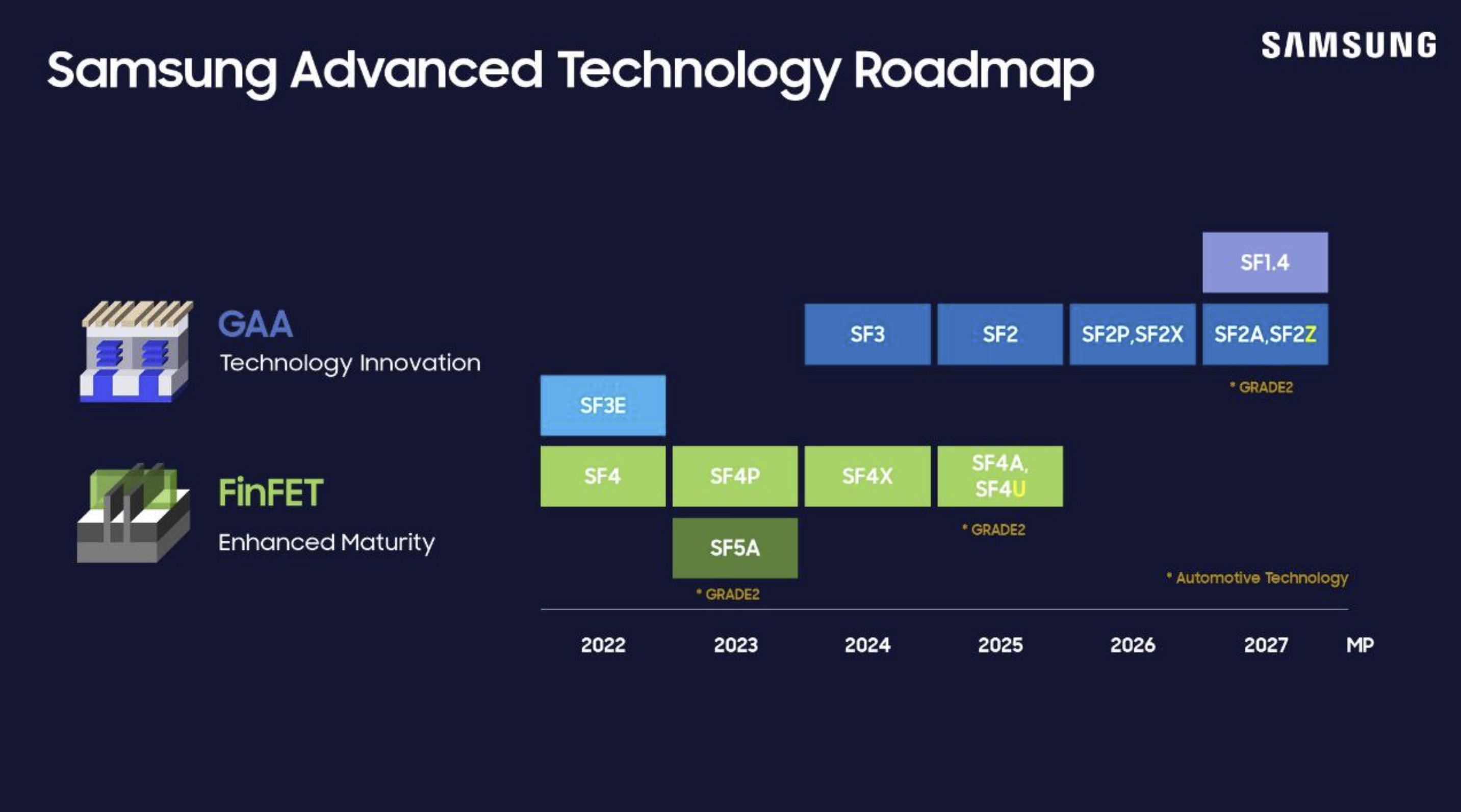
Market Implications and Competitive Dynamics
The divergent approaches of these three foundries reflect broader trends in the semiconductor industry:
TSMC's execution excellence has allowed it to maintain its leadership position, particularly in serving the most demanding customers like Apple and AI chip manufacturers. The company's segmentation strategy enables it to capture a wide range of market segments without forcing all customers onto its most expensive nodes.
Intel's aggressive technological roadmap represents a high-risk, high-reward strategy. By combining multiple advanced technologies (GAA transistors, BSPDN, High-NA EUV) in each node, Intel hopes to leapfrog competitors. However, the cancellation of 20A demonstrates the challenges of maintaining such an aggressive pace.
Samsung's yield-focused approach suggests a more conservative strategy that prioritizes stability and manufacturability over bleeding-edge performance. This approach may limit Samsung's ability to compete at the absolute leading edge but could position it well in high-volume applications where reliability and cost are paramount.
The foundry landscape is also becoming increasingly segmented by application. While all three companies compete for leading-edge logic applications, they are pursuing different strategies for emerging markets like AI accelerators, automotive chips, and IoT devices. TSMC's automotive-specific nodes lagging by 1-2 generations compared to its leading-edge nodes reflect the different requirements of this market segment, where reliability and longevity are more critical than absolute performance.
As the industry approaches the 1.4nm node and beyond, the competitive dynamics will continue to evolve. The ability to combine multiple advanced technologies—GAA transistors, backside power delivery, and High-NA EUV lithography—while maintaining high yields and reasonable costs will determine which foundry emerges as the leader in the next generation of process technologies.
Comments
Please log in or register to join the discussion