
NEO Semiconductor has successfully validated its 3D X-DRAM technology through proof-of-concept testing, demonstrating high-performance memory characteristics using existing 3D NAND manufacturing processes. The company has secured strategic funding led by tech industry veteran Stan Shih to develop this potential alternative to High Bandwidth Memory (HBM) for AI processors.
NEO Semiconductor announced on April 23rd that its 3D X-DRAM technology has successfully passed proof-of-concept (POC) validation, marking a significant milestone in the evolution of memory architectures for artificial intelligence workloads. The company simultaneously secured a strategic investment led by Stan Shih, founder and former Chairman and CEO of Acer, and a board director of TSMC for over two decades, providing the financial foundation to advance this promising memory technology.
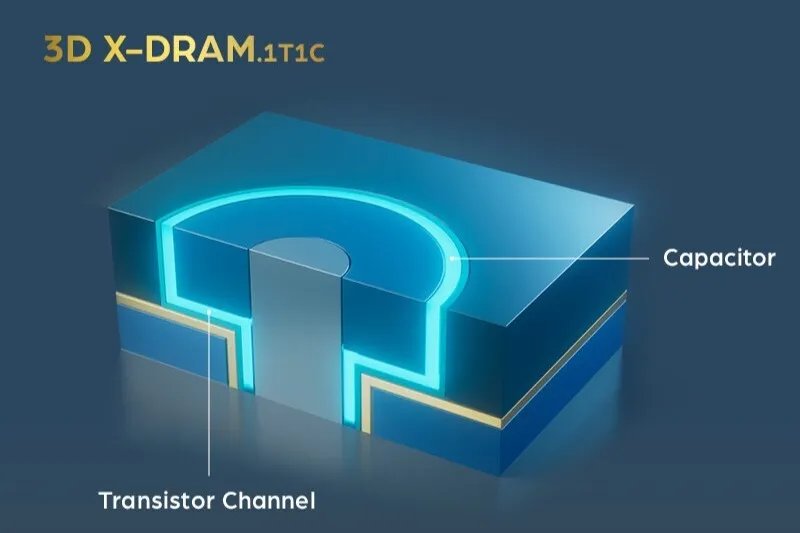
At the core of this announcement is NEO Semiconductor's 3D X-DRAM technology, which represents a new class of DRAM designed to overcome conventional memory scaling limitations through a vertically stacked architecture optimized for higher density, lower power consumption, and improved performance in AI-driven applications. Unlike traditional approaches that have struggled with diminishing returns at smaller process nodes, NEO's innovation leverages existing manufacturing infrastructure to achieve potentially revolutionary results.
Technical Validation and Performance Metrics
The proof-of-concept chips, fabricated and tested at Taiwan's National Institutes of Applied Research - Taiwan Semiconductor Research Institute (NIAR-TSRI) in collaboration with National Yang Ming Chiao Tung University, demonstrated impressive electrical characteristics that position 3D X-DRAM as a compelling alternative to current memory solutions:
- Read/write latency: under 10 nanoseconds
- Data retention: over 1 second at 85°C (claimed 15× improvement over JEDEC standard)
- Bit-line disturbance: over 1 second at 85°C
- Word-line disturbance: over 1 second at 85°C
- Endurance: greater than 10¹⁴ cycles
These performance metrics suggest significant advantages over conventional DRAM architectures, particularly in the areas of data retention and endurance, which are critical for AI workloads that involve massive datasets and complex computational patterns.
Manufacturing Innovation: Leveraging 3D NAND Processes
Perhaps most significant is that NEO's 3D X-DRAM architecture draws heavily on 3D NAND manufacturing techniques. According to the company, the POC chips were produced using mature 3D NAND processes, including existing equipment and materials. This approach addresses one of the primary constraints in advanced memory development: not design innovation, but fabrication cost and process compatibility.
"These results validate a new scaling path for DRAM," said Andy Hsu, Founder & CEO of NEO Semiconductor. "We believe this technology can enable significantly higher density, lower cost, and improved energy efficiency for the AI era. By leveraging established 3D NAND manufacturing processes and ecosystem, we aim to bring 3D DRAM to reality sooner."

Differentiation from HBM Architecture
The 3D X-DRAM technology emerges in a context where AI workloads are placing unprecedented demands on memory systems. While GPU compute performance has scaled dramatically over the past decade, memory bandwidth—the rate at which data can be fed to processors—has become a limiting factor in large-scale AI training and inference systems. This has driven widespread adoption of High Bandwidth Memory (HBM), a vertically stacked DRAM architecture integrated close to GPUs.
However, HBM presents several challenges:
- Complex 3D stacking and bonding requirements
- High manufacturing costs
- Limited scalability due to thermal and mechanical constraints
3D X-DRAM offers an alternative approach. While both technologies use vertical stacking concepts, they stack different elements in different ways:
- HBM: Stacks multiple finished DRAM dies on top of each other, then connects them with through-silicon vias (TSVs) and places them beside/near a GPU or CPU on an interposer
- 3D X-DRAM: Builds memory cells in a 3D NAND-like monolithic vertical structure, where layers are fabricated as part of the memory array itself rather than stacking separate packaged DRAM dies
This fundamental difference in architecture could potentially offer better cost structure, higher density, and improved thermal characteristics compared to HBM solutions.
Market Context and Competitive Landscape
NEO Semiconductor's announcement comes amid intensifying competition in the AI memory space. Just a day before NEO's announcement, industry reports highlighted SAIMEMORY and its ZAM architecture, backed by SoftBank and Intel with Japanese government support, pursuing similar goals on a parallel track.
The broader industry context is that conventional DRAM scaling is approaching physical limits, prompting increased exploration of vertical alternatives. TechInsights' Jeongdong Choe described NEO's results as a "significant milestone" in this shift toward 3D memory architectures.
"The successful proof-of-concept not only demonstrates the potential of innovative memory architectures, but also confirms the feasibility of implementing advanced memory technologies using mature processes," said Jack Sun, Senior Vice President of NYCU and Dean of IAIS, and former CTO of TSMC. "This collaboration among NEO, NYCU IAIS, and NIAR-TSRI further underscores the value of industry–academia partnerships in accelerating innovation from concept to practical implementation."
Strategic Implications and Path Forward
With the successful validation of its proof-of-concept and securing strategic funding, NEO Semiconductor is positioned to advance 3D X-DRAM toward commercialization. The company has indicated it is actively engaging with leading global memory and semiconductor companies on potential co-development opportunities, suggesting a licensing and partnership model rather than attempting to build its own manufacturing capabilities.
This approach mirrors successful strategies in the semiconductor industry where innovative IP companies partner with established manufacturers to bring new technologies to market. Given that NEO's technology leverages existing 3D NAND processes, the potential for faster adoption compared to entirely novel memory architectures is significant.
However, it is crucial to note that this remains a proof of concept, not a production-ready memory chip. The road from validated POC to commercial volume is long—historically littered with the remains of promising memory technologies that never made it out of the lab. Success will depend on several factors, including:
- Ability to scale the technology to production volumes
- Cost competitiveness compared to established memory solutions
- Performance validation across diverse workloads
- Industry adoption by major system and chip manufacturers
As AI continues to drive demand for higher memory bandwidth and capacity, innovations like 3D X-DRAM could play a crucial role in enabling the next generation of AI systems. If NEO Semiconductor can successfully transition this technology from lab to fab, it may represent a significant advancement in memory architecture for AI applications, potentially reducing costs while improving performance characteristics that matter most for large-scale machine learning workloads.
Comments
Please log in or register to join the discussion