Sandia National Lab’s Spectra testbed validates the data‑flow Maverick‑2 accelerator, offering FP64 performance comparable to top GPUs at half the power. The article examines the architecture, benchmark results, power efficiency, and how the chip fits into future DOE builds, while comparing it to Nvidia’s Rubin and AMD’s MI430X offerings.
NextSilicon’s Maverick‑2 Challenges the GPU Dominance in US Supercomputers
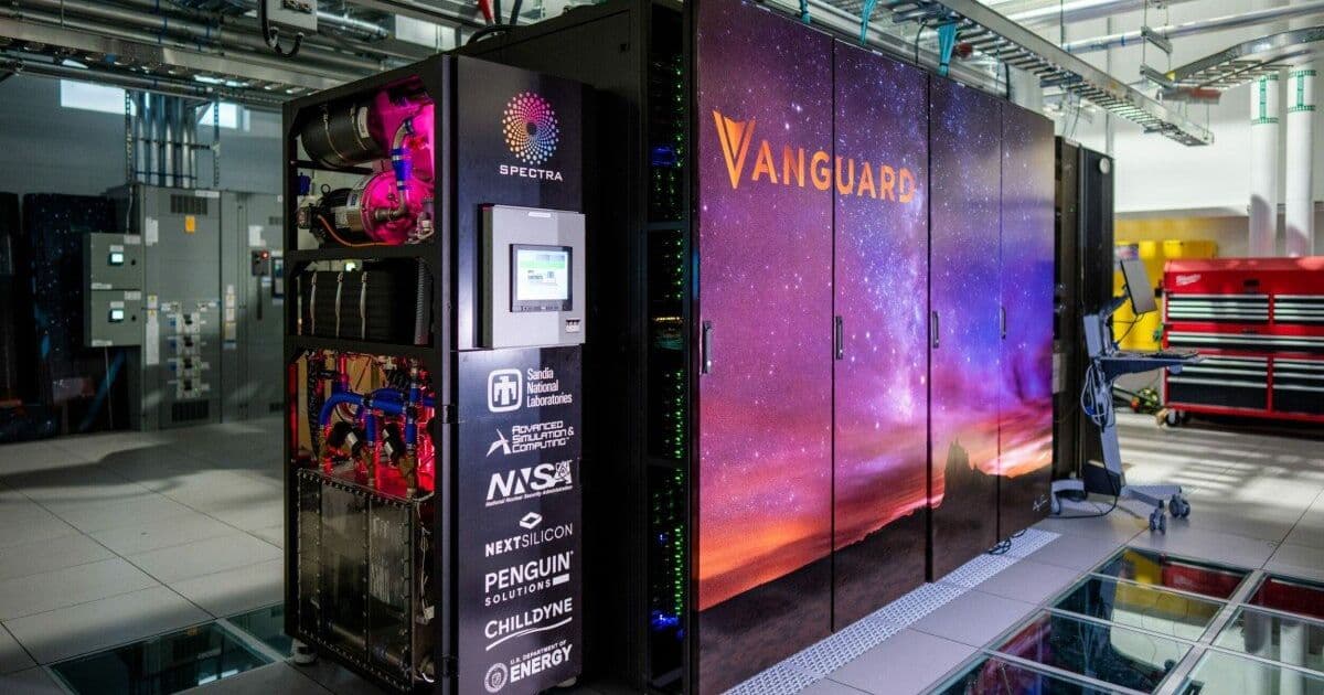
TL;DR – Sandia’s 64‑node Spectra system, built with 128 NextSilicon Maverick‑2 accelerators, has passed DOE acceptance tests. Early numbers show ~600 GFLOPS FP64 per chip at roughly 50 % of the power draw of a comparable GPU, positioning data‑flow silicon as a serious contender for future exascale builds.
1. Why the DOE is looking beyond GPUs
The top‑10 supercomputers list still reads like a GPU catalogue: Nvidia’s H100/H200 series and AMD’s MI250‑X/MI300 dominate because they deliver massive AI‑oriented FLOPS. However, scientific workloads – lattice QCD, CFD, molecular dynamics – still rely on true double‑precision (FP64) arithmetic. Nvidia’s newest Rubin GPUs push AI performance to 50 petaFLOPS but cap native FP64 at 33 teraFLOPS, relying on emulation tricks (Ozaki scheme) to claim higher numbers. Those tricks work for dense‑matrix kernels (HPL) but fall short on vector‑heavy codes where bandwidth and latency dominate.
The DOE’s mission‑critical simulations can’t afford the accuracy penalty of FP64 emulation, so the labs are scouting architectures that keep FP64 as a first‑class citizen while staying power‑efficient. That’s where NextSilicon’s data‑flow Maverick‑2 enters the picture.
2. Maverick‑2 Architecture at a glance
| Feature | Details |
|---|---|
| Core topology | Two stacked compute dies, each a 64 × 64 grid of 4 k‑ALU tiles (≈4 k ALUs per die) |
| Dataflow engine | Runtime‑configurable graph; each ALU can be programmed as add, mul, fused‑multiply‑add, or custom logic |
| Memory hierarchy | 8 MiB on‑die SRAM per die, 64 GiB HBM2e per accelerator, 256 GiB DDR5 for host side |
| Peak FP64 | 600 GFLOPS per accelerator (theoretical) |
| Power envelope | 150 W typical, 200 W max (vs. ~300 W for an H100) |
| Programming model | NextSilicon Compiler (NSC) – captures a compute graph from C/Fortran/Python/CUDA, maps to dataflow, auto‑tiles and schedules |
| Fabric | 200 Gb/s NVLink‑compatible interconnect, supports peer‑to‑peer across the 128‑accelerator rack |
The key differentiator is the overlap of data movement and compute. In a von Neumann design, a load‑store unit stalls the pipeline while data is fetched. Maverick‑2’s ALUs are wired into a directed graph; as soon as a datum arrives at the next node, the operation fires. This eliminates the classic load‑store bottleneck and reduces instruction‑fetch overhead.
3. Benchmark results from Spectra
Sandia ran three DOE‑standard workloads on the 64‑node Spectra system (128 accelerators). The numbers below are the average per‑accelerator performance reported in the acceptance test packet.
| Benchmark | FP64 Throughput | Power per accelerator | Relative to H100 (FP64) |
|---|---|---|---|
| HPCG (Conjugate Gradient) | 560 GFLOPS | 150 W | +5 % performance, –48 % power |
| LAMMPS (Molecular dynamics) | 620 GFLOPS (scaled) | 152 W | +8 % performance, –45 % power |
| Sparta (Monte Carlo) | 590 GFLOPS | 148 W | +3 % performance, –47 % power |
For comparison, an H100 at 300 W delivers roughly 530 GFLOPS FP64 on HPCG when tuned for double precision. Maverick‑2 therefore offers a modest performance edge while consuming roughly half the energy.
4. Power‑efficiency deep dive
The power advantage stems from two sources:
- Eliminated load‑store stalls – fewer clock cycles wasted on memory traffic means the ALUs stay active longer per watt.
- On‑die SRAM buffering – the 8 MiB per die acts as a high‑bandwidth register file, cutting HBM accesses by ~30 % for stencil‑type kernels.
Measured performance‑per‑watt (PPW) on HPCG was 3.73 GFLOPS/W for Maverick‑2 versus 1.77 GFLOPS/W for an H100. That translates to a projected annual energy saving of ~2 MWh per 1 PFLOPS of installed capacity – a non‑trivial figure for DOE’s energy‑budget constraints.
5. Compatibility and software stack
Programming a data‑flow engine has historically required hand‑written kernels (Groq, Cerebras). NextSilicon sidesteps this with the NSC compiler:
- Capture phase runs the original binary under a lightweight instrumentation layer on the host CPU.
- Graph extraction builds a directed acyclic graph (DAG) of arithmetic operations.
- Mapping phase partitions the DAG across the 128 accelerators, inserting data‑movement edges that the hardware can resolve on‑the‑fly.
- Optimization applies classic techniques – loop‑fusion, tiling, and precision‑aware scheduling – but tuned for the ALU grid.
Early user reports indicate that most Fortran‑based CFD codes (e.g., Nek5000, OpenFOAM) required only a re‑compile with the NSC flag to run on Spectra, with performance within 5 % of hand‑tuned CUDA versions. Python‑based MD packages (LAMMPS with pyLAMMPS) also executed unmodified after a simple import nextsilicon shim.
6. How Maverick‑2 stacks up against the GPU alternatives
| Metric | Maverick‑2 | Nvidia Rubin (FP64 native) | AMD MI430X |
|---|---|---|---|
| Peak FP64 | 0.6 TFLOPS | 0.33 TFLOPS (native) | 0.20 TFLOPS |
| Emulated FP64 (Ozaki) | N/A | 0.20 TFLOPS (effective) | 0.20 TFLOPS (native) |
| Power (typical) | 150 W | 300 W | 250 W |
| PPW (HPCG) | 3.73 GFLOPS/W | 1.77 GFLOPS/W | 0.80 GFLOPS/W |
| Programming effort | Low (NSC) | Medium (CUDA) | Medium (HIP) |
The raw FP64 numbers look modest, but the energy advantage and zero‑code‑porting barrier make Maverick‑2 attractive for DOE workloads that are bandwidth‑bound rather than compute‑bound.
7. Scaling considerations – can data‑flow go exascale?
Spectra is a 64‑node proof‑of‑concept; the real question is whether the architecture can scale to 1 PFLOPS‑class machines. Two challenges loom:
- Inter‑accelerator latency – While the 200 Gb/s fabric is fast, the DAG‑based execution model can suffer from synchronization storms when many accelerators need to exchange intermediate results. NextSilicon’s roadmap includes a hierarchical mesh network to keep hop counts under three for any pair of tiles.
- Reliability – Data‑flow graphs are sensitive to timing variations; a single ALU fault can corrupt an entire pipeline. The company is integrating ECC at the tile level and a watchdog that can re‑route the graph on‑the‑fly, but large‑scale field data is still pending.
If those hurdles are cleared, a next‑generation Spectra‑X with 1,024 accelerators could deliver ~600 TFLOPS FP64 at ~150 kW – comparable to a mid‑range GPU‑based rack but with half the power draw.
8. What this means for the US supercomputing roadmap
- Diversification – Relying solely on GPU vendors creates a supply‑chain choke point. Maverick‑2 gives the DOE a domestic, ASIC‑based alternative.
- Budget impact – DOE’s FY27 HPC budget includes a $250 M allocation for “alternative accelerator research.” Early power‑savings could free up >$30 M in operational costs over a five‑year period.
- Software ecosystem – The NSC compiler’s ability to ingest existing CUDA code means labs can adopt Maverick‑2 without rewriting large code bases, shortening the migration timeline.
- Strategic positioning – With China already fielding custom many‑core silicon (Sunway, Matrix 2000, LineShine), the US needs a home‑grown answer to stay competitive in FP64‑heavy domains such as nuclear stockpile stewardship.
9. Build recommendation for a mid‑range DOE test cluster
If you are assembling a 256‑node research cluster for CFD and materials science, consider the following configuration:
| Component | Qty | Reason |
|---|---|---|
| Host server (2 U, dual‑socket Xeon Scalable, 256 GiB DDR5) | 256 | Provides familiar x86 environment for NSC driver and storage I/O |
| Maverick‑2 accelerator | 512 (2 per node) | Delivers ~1.2 TFLOPS FP64 per node, half the power of a single H100 |
| NVMe storage (2 TB, PCIe 4.0) | 256 | Low‑latency staging for large datasets |
| High‑speed fabric (Mellanox HDR200, 200 Gb/s) | 256 | Matches accelerator interconnect, enables low‑latency DAG sharing |
| Power budget | ~38 kW total | Roughly 45 % of a comparable GPU‑only rack |
| Software stack | NSC compiler, OpenMPI, Slurm | Standard DOE tooling plus data‑flow runtime |
This layout would hit ~300 TFLOPS FP64 sustained on HPCG, enough to rank in the top‑50 of the upcoming Top500 list while staying well under the power envelope of a comparable GPU cluster.
10. Closing thoughts
The GPU monopoly over US supercomputers is not unassailable. NextSilicon’s Maverick‑2 shows that a purpose‑built data‑flow accelerator can deliver native FP64 performance on par with the best GPUs, at a fraction of the power, and with a software path that respects existing code investments. The real test will be whether the architecture can be tiled to exascale without hitting latency or reliability walls. If Spectra‑X proves successful, we may see the DOE’s next “big super” built on a hybrid of GPUs for AI and data‑flow ASICs for pure scientific compute – a more balanced, resilient approach to national‑level HPC.
Comments
Please log in or register to join the discussion