A developer's race to build an AI accelerator and debug infrastructure in just 14 days highlights both the power and limitations of accessible chip design platforms.
The open-source silicon movement continues lowering barriers to custom chip design, but a recent experimental shuttle reveals intriguing patterns about what happens when fabrication becomes nearly free. Tiny Tapeout's experimental program—offering GlobalFoundries 180nm fabrication at zero cost to veteran designers—has become a testing ground not just for new process nodes, but for extreme design methodologies. One participant's sprint to tapeout in just two weeks exemplifies how tooling maturity enables previously unthinkable timelines, while exposing enduring constraints.
The Experimental Playground
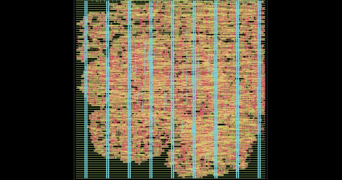
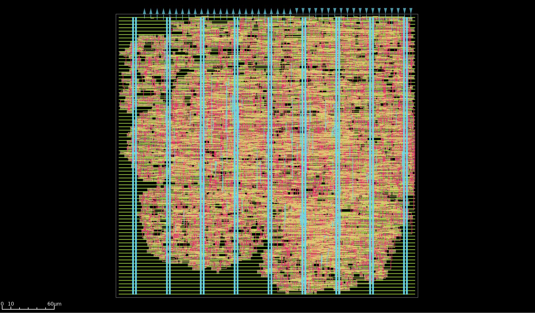
Tiny Tapeout's experimental shuttles operate under unique conditions: participation requires prior tapeout experience, tools are less stable, and designs share resources without full isolation. Crucially, submissions are free—making silicon area effectively a free commodity. This economic shift leads to fascinating behavioral changes. As one designer notes: "In practice, this makes area effectively free, explaining the higher occurrence of absolutely massive designs being submitted." The program intentionally accepts risk; participants understand their chips might fail due to tooling issues beyond their control.
{{IMAGE:2}}
The Two-Week Crucible
Against this backdrop, developer Essenceia accepted a daunting challenge: tape out a dual-purpose ASIC featuring both a 2x2 systolic array matrix multiplier (for AI workloads) and a custom JTAG debug interface in just 14 days. After accounting for post-previous-project recovery, actual design time shrank to 10 days. Such timelines would be untenable in commercial settings but become feasible through three key enablers:
- Toolchain maturity: LibreLane and OpenROAD's automated flows enabled "no-human-in-the-loop" implementation
- Pre-built infrastructure: Custom workflows like single-command FPGA emulation (
make fpga_prog debug=1) - Protocol leverage: Existing standards like JTAG with robust software support (OpenOCD)
The true bottleneck became human endurance, humorously documented as "homo electro-engineerus observed in its natural habitat... surviving exclusively on a diet of coffee and smoked ham."

Systolic Arrays Meet I/O Walls
The systolic array design prioritized compute/memory efficiency—critical for AI accelerators where data movement dominates power consumption. As the developer explains: "SRAM accesses cost time and significant power, while DRAM accesses cost eternities... Compute operations, even 64-bit floating point multiplications, are by comparison, cheap." Yet Tiny Tapeout's constraints forced hard compromises:
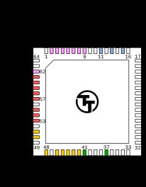
- Only 8 input/output pins with uncharacterized max frequency (~50MHz assumed)
- No SRAM due to experimental shuttle limitations
- Self-imposed size limits (2x2 array) to preserve area for others
These restrictions highlight a persistent gap: while open-source tools democratize design, I/O bandwidth remains a stubborn frontier. The solution? Clever buffering and controller logic to serialize parallel data.
Comments
Please log in or register to join the discussion