This article details the Neodyme security research team's process for extracting firmware from a Potensic Atom 2 drone, a process that involved physical chip desoldering, raw data dumping, and a deep dive into the complex world of Error Correction Codes (ECC). The team navigated bit errors, non-standard data layouts, and the need to brute-force cryptographic parameters to successfully reconstruct a usable firmware image, setting the stage for vulnerability analysis.
In the world of hardware security research, gaining a copy of a device's firmware is the foundational step. It's the Rosetta Stone that allows a researcher to translate the device's binary operations into understandable logic, revealing its secrets, potential backdoors, and vulnerabilities. For the Potensic Atom 2 drone, a device that presents a familiar silhouette to DJI's popular Mini series, this seemingly simple goal became a multi-layered puzzle of hardware manipulation and cryptographic deduction. This is the story of how we at Neodyme dismantled this drone, bit by bit, to get at the code running its core.
The Initial Hurdles: A Trifecta of Failed Approaches
Our goal was straightforward: obtain a copy of the Atom 2's firmware. We explored several common avenues before committing to the most invasive one. The first, and most elegant, approach would be to simply download the firmware update from the manufacturer. However, this path was quickly blocked; the update process required valid, registered serial numbers for both the drone and its remote control, and the firmware files themselves were encrypted. Without the decryption key or the logic to derive it, this was a dead end.
Next, we looked for exposed debug interfaces like JTAG or UART. These ports can sometimes provide a direct pipeline for reading or writing to a device's memory. A thorough inspection of the Atom 2's mainboard, however, revealed no such convenient access points. The manufacturer had clearly taken steps to secure these interfaces.
With the software and interface approaches exhausted, we were left with the hardware method: physically removing the NAND flash memory chip and reading its contents directly. This is a high-risk, high-reward strategy. It requires precision soldering and carries the risk of destroying the chip or the board. Furthermore, we had to consider if the effort would even be worthwhile. Some modern devices, like smartphones, encrypt their storage at a hardware level, meaning a raw dump of the NAND chip would be nothing but an unintelligible block of ciphertext. Fortunately, a preliminary analysis of the Atom 2's specifications suggested this was not the case, giving us the green light to proceed.
The Physical Extraction: Soldering into the Core
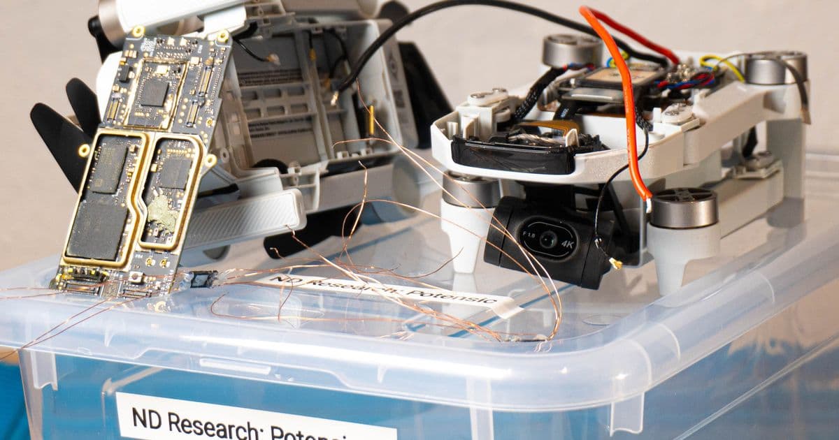
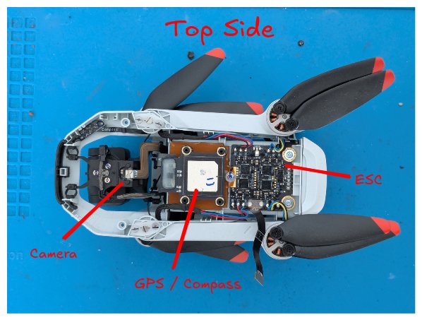
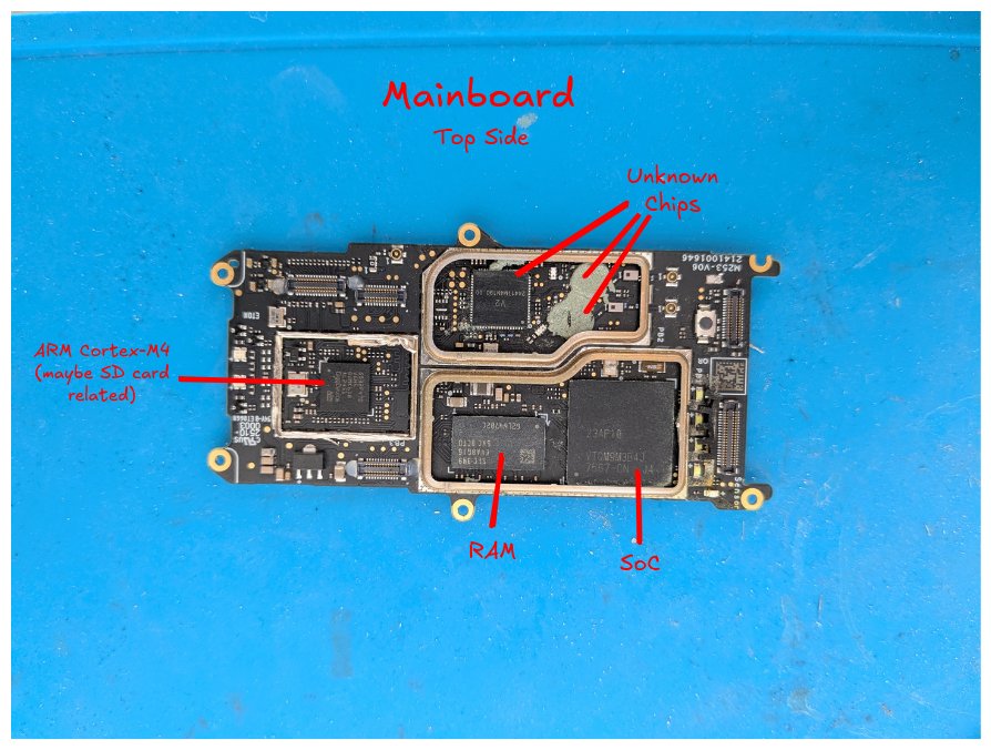
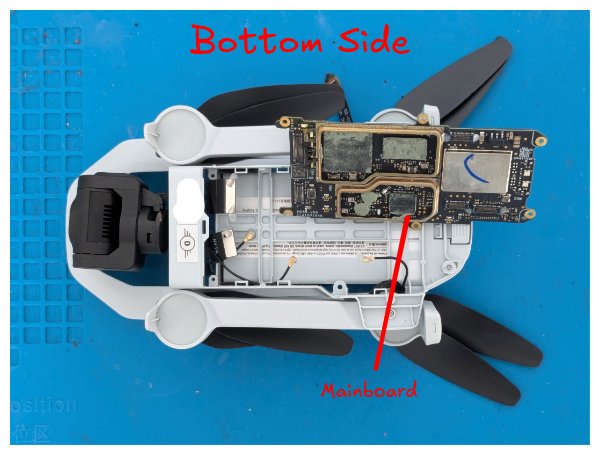
Our first task was to identify the target. The drone's mainboard was shielded by several metal RF covers, which we carefully pried off. By cross-referencing the markings on the various chips with their corresponding datasheets, we built a profile of the drone's brain. The central component is a System-on-a-Chip (SoC), likely a HiSilicon model designed for mobile camera applications, which makes sense given the drone's 4K video capabilities. Adjacent to it are RAM chips and, most importantly for our mission, the NAND flash chip: an MXIC MX35UF4GE4AD.
With the chip identified, the delicate work of removal began. The chip was not just soldered to the board but also secured with epoxy, a common technique to deter exactly what we were attempting. After carefully cutting around the chip's perimeter with a sharp knife and applying heat and flux, we successfully lifted the NAND chip from the board. Our next step was to prepare it for reading. The chip used a standard SPI (Serial Peripheral Interface) protocol. We painstakingly soldered tiny copper wires to each of the chip's pins—CS, SI, SO, SCLK, and the rest—and connected them to an ESP32 microcontroller.
The Raw Dump: A Flood of Data and Errors
Using a custom script on the ESP32, we began reading the chip's contents. The process yielded a 544 MiB raw dump. A quick analysis with binwalk confirmed we were on the right track; the tool identified UBIFS file systems, the type of storage architecture commonly used in embedded Linux devices. Our initial excitement was tempered, however, when we tried to extract the files. The process failed, indicating the data was corrupted.
This led us to a critical discovery: random bit flips. Reading data from a chip using hand-soldered wires on a breadboard is inherently noisy. We ran the dump process three times and compared the results. The MD5 hashes were different each time, proving that our reading process was introducing errors. To solve this, we implemented a majority voting algorithm: for every bit position, we took the value that appeared in at least two of the three dumps. This corrected for our transmission errors, but it wasn't the end of our problems.
The Core Challenge: Untangling Error Correction Codes (ECC)
Even after majority voting, the extracted file system remained broken. The issue wasn't just our reading process; it was the fundamental nature of NAND flash. This storage medium is inherently unreliable; bits can decay over time. To compensate, manufacturers and SoC designers implement Error Correction Codes (ECC). Extra bytes, called "out-of-band" (OOB) bytes, are stored alongside the user data. These bytes contain parity information that allows the system to detect and correct a certain number of bit flips on the fly.
Our initial assumption was simple: each 4096-byte page of user data was followed by 256 bytes of ECC data. This assumption was quickly proven wrong when we found readable strings within the OOB data and saw that text within the user data was abruptly cut off. This meant the data and ECC were interleaved in a more complex pattern.
The breakthrough came when we found the datasheet for the drone's HiSilicon SoC. It described the chip's specific ECC layout, which was fragmented across the page. By following this diagram, we could slice the raw dump into its constituent user data, ECC, and control sections, and then reassemble just the user data. This corrected the structure, and binwalk once again recognized a UBIFS image. But the file system was still too corrupt to mount.
The final piece of the puzzle was that the NAND chip itself contained bit flips that had occurred during writing or storage. The SoC's ECC algorithm was designed to fix these, but we had stripped the ECC data away. We now faced a chicken-and-egg problem: to recover the user data, we needed to implement the ECC algorithm, but to do that, we first had to reverse-engineer the exact parameters of the algorithm itself.
The Final Frontier: Brute-Forcing the ECC Algorithm
We knew we were dealing with a BCH (Bose-Chaudhuri-Hocquenghem) code, a common type of ECC. From the datasheet and our analysis of the data layout, we could deduce some parameters: we had 224 parity bits (28 bytes per 1028-byte chunk of user data) and a correction capacity of up to 16 bit flips per chunk. However, the datasheet was silent on the other crucial parameters: the specific primitive polynomial used, and any pre- or post-processing transformations applied to the data before the parity was calculated.
To find these missing parameters, we devised a brute-force attack. The strategy was to:
- Find a "clean" section of user data from our dump—one that we assumed had no bit flips.
- Iterate through all possible combinations of common transformations (like inverting bits, reversing byte order, etc.).
- For each combination, iterate through all possible primitive polynomials of the correct degree.
- For each candidate, generate our own ECC and check if it matched the known ECC from the chip.
After a 22-second search, our script found a match. The correct parameters were a primitive polynomial of 17475, with both pre- and post-transformations consisting of reversing the bit order and then inverting all bits.
With the full ECC algorithm now understood, we could finally process the entire firmware dump. Our final script iterated through every page of the flash memory, applying the correct ECC layout and correcting bit flips as it went. The result was a clean, usable firmware image. A subsequent run with ubi_reader successfully extracted two of the three file systems, providing us with the files needed to begin the next phase of our research.
This journey from a physical chip to a clean firmware image demonstrates that reverse engineering is often a process of peeling back layers of abstraction. It's not just about code, but about understanding the hardware, the data layout, and the mathematical principles that hold it all together. With a working firmware in hand, we can now begin the true hunt for vulnerabilities, which we will detail in the second and final part of this series.
Comments
Please log in or register to join the discussion