
Baltazar Studios chronicles a ten‑chapter odyssey that begins with a power outage in Austin and ends with a fully functional scientific calculator built on a modest FPGA. The series explores the early motivation, the often‑unseen path‑finding phase, rigorous numerical methods, a cross‑environment testing framework, hardware prototyping, a bespoke CPU architecture, microcode development, PCB realization, precision enhancements, and the final reflections on a 1,593‑cell design.
Designing an FPGA Calculator from Scratch – A Journey Through Hardware, Software, and Numerical Theory
Thesis
The project described by Baltazar Studios is more than a hobbyist’s recreation of an HP‑41CV; it is a case study in how a single‑person engineering effort can traverse the entire product development stack—conceptual spark, algorithmic rigor, verification framework, silicon implementation, and iterative refinement—while remaining entirely free‑tool driven. The narrative demonstrates that, with disciplined methodology, a modest Cyclone II FPGA can host a full‑featured scientific calculator that respects 16‑digit BCD precision, all within a few thousand logic cells.
1. The Origin Story – From Blackout to Inspiration
In February 2021 a grid failure left Austin residents dependent on a gas fireplace and a flaky cellular link. The author, clutching an HP‑41CV, felt the tactile satisfaction of a classic RPN calculator and wondered what it would take to recreate that experience on an FPGA. This personal anecdote sets the emotional tone: engineering as a response to scarcity, not merely curiosity.
2. Pathfinding – The Unwritten Phase
Before any schematic appears, the author engages in a series of throw‑away experiments: quick Verilog sketches, Python prototypes, and even breadboard mock‑ups. The purpose is to discover dead ends early—whether the chosen memory model can support BCD mantissas, or if the timing of a keypad matrix can be met with the target device. The chapter emphasizes that this exploratory work, though rarely documented, is the crucible where feasibility is either forged or discarded.
3. Practical Numerical Methods – From Theory to 16‑Digit Accuracy
A central technical hurdle is implementing transcendental functions (tan, ln, exp, sqrt) using only addition, subtraction, and multiplication. The author references a prior post that proves the feasibility via series expansions and CORDIC‑style iterations, then proceeds to a verified reference implementation capable of delivering 16 decimal digits. The implementation relies on:
- Fixed‑point 64‑bit representations to avoid floating‑point units.
- Guard digits and sticky bits to preserve precision during intermediate steps.
- Banker's rounding to ensure unbiased results across repeated operations.
The result is a library of functions that can be directly mapped to the FPGA’s ALU.
4. The Framework – One RTL, Four Testbeds
Testing hardware that does not yet exist is a paradox solved by a unified simulation environment. The author builds a Verilog test harness that can be compiled for:
- ModelSim – signal‑level waveform inspection.
- Verilator – cycle‑accurate C++ model for fast regression.
- Qt – a desktop GUI that mimics the calculator’s keypad and OLED, exposing a console for debugging.
- WebAssembly – a browser‑based emulator that runs the same RTL without modification.
All tools are open source, reinforcing the project’s accessibility. The framework ensures that any bug discovered in the Qt prototype is automatically reproduced in the hardware simulation, dramatically reducing the iteration cycle.
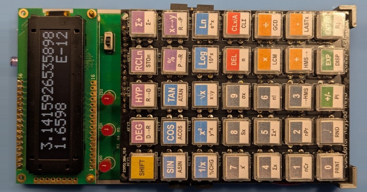
5. The Hardware – From Schematic to First PCB
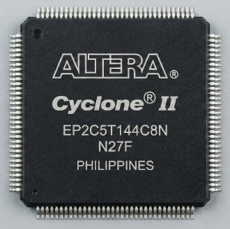
The first physical prototype consists of a keypad matrix and a 128×32 OLED display connected to an Altera Cyclone II EP2C5 development board via a ribbon cable. The author uses a browser‑based schematic editor (e.g., KiCad in the cloud) to design the board, then orders a two‑layer PCB for under $5. The assembly process highlights practical concerns:
- Signal integrity on the ribbon cable—length matching and proper termination.
- Power sequencing for the OLED, requiring a soft‑start to avoid flicker.
- Debounce logic implemented in Verilog to clean noisy keypad contacts.
6. Designing the CPU – A Nibble‑Addressable BCD Machine
Standard CPUs lack the nibble‑addressable memory layout required for a 16‑digit BCD mantissa. The author therefore designs a custom 12‑bit fixed‑length instruction set with a Harvard architecture. Highlights include:
- 14 ALU operations, among them BCD‑adjust instructions borrowed from the 8086 (DA, AAA, AAS) to simplify decimal correction after addition or subtraction.
- Micro‑coded control stored in a small ROM, allowing the instruction set to evolve as new arithmetic functions are added.
- Iterative ISA development—each new instruction is written, verified in Verilator, and then used to expose shortcomings in the existing microcode.
7. Writing Microcode – From C++ Prototypes to Real Execution
The earlier C++ reference implementation becomes the source of truth for microcode development. Each assembly routine mirrors a proven software function, guaranteeing functional equivalence. The author introduces a tiny scripting interpreter that tokenizes expressions like y^x into six micro‑operations, demonstrating how higher‑level language features can be built atop a minimal instruction set.
Debugging is performed in the Qt simulator, where breakpoints, register watches, and step‑through execution replace the traditional "printf" debugging strategy that is unavailable in microcode.
8. From Dev Board to a Real Device – PCB, Enclosure, and Programming Interfaces
Transitioning from a development board to a self‑contained device involves:
- Designing a custom PCB that hosts the FPGA, power regulation, keypad, and OLED on a single board.
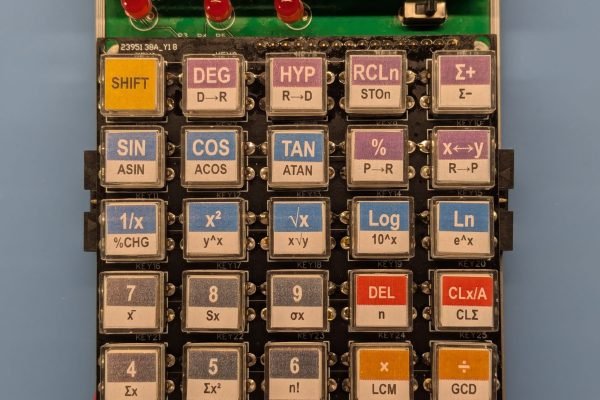
- 3D‑printing an enclosure that mimics the HP aesthetic, complete with yellow‑and‑red keycaps.
- Providing JTAG for rapid development cycles and Active Serial for persistent flash programming, ensuring the edit‑synthesize‑test loop remains tight even after the board is sealed.
9. Chasing the Last Digit – Precision Overhaul (2025 Rewrite)
The initial 2021 implementation achieved about 12 correct digits, insufficient for a true 16‑digit BCD calculator. The 2025 rewrite introduces:
- Guard‑digit and sticky‑bit tracking throughout the arithmetic pipeline.
- Banker’s rounding at every stage to avoid cumulative bias.
- A full trigonometric suite (sin, cos, tan, arcsin, etc.) built on range‑reduction and polynomial approximations.
- Ten user‑accessible STO/RCL registers for temporary storage.
- A hardware LFSR random‑number generator validated against thousands of reference vectors.
- Interrupt handling—a modest addition that consumes only 24 logic cells but showcases the flexibility of the design.
The revised engine fits in 1,593 logic cells, representing roughly 35 % of the EP2C5’s capacity.
10. It Works! – Reflections on a 1,593‑Cell Scientific Calculator
The final chapter tallies the achievements: a fully functional scientific calculator, a complete development pipeline, and a deep understanding of both digital design and numerical analysis. The author candidly notes remaining pain points—keypad feel, the difficulty of soldering a TQFP‑144, and the unexpected bulk when moving from bench‑top to portable. Nonetheless, the project stands as proof that a disciplined, end‑to‑end approach can yield sophisticated hardware without corporate resources.
Implications for the Maker Community
- Methodology over tools – The same Verilog source runs across four environments, illustrating that a well‑structured test harness can replace expensive hardware debuggers.
- Precision matters – Implementing BCD arithmetic with proper rounding and guard digits is feasible on tiny FPGAs, opening doors for other decimal‑oriented applications such as financial calculators.
- Open‑source viability – Every component—from schematic editor to simulation suite—is freely available, encouraging replication and extension.
Counter‑Perspectives
Some may argue that a modern microcontroller with built‑in floating‑point could achieve the same functionality with less effort. While true for raw performance, the FPGA approach offers deterministic timing, true parallelism for the ALU, and an educational platform that forces the designer to confront low‑level numeric representation—a valuable experience that high‑level MCUs abstract away.
For readers interested in the full series, each chapter is linked from the original Baltazar Studios site, and the Verilog source is hosted on the project's GitHub repository.
Comments
Please log in or register to join the discussion