
In the early 1970s IBM’s Project SWIFT built a fully automated wafer fab that could turn a blank wafer into a working RAM chip in a single day—a speed that still outpaces modern fabs. Led by Bill Harding, the five‑sector line introduced concepts such as single‑wafer processing, centralized computer control, air‑track handling and real‑time process monitoring, many of which are now standard in today’s billion‑dollar semiconductor plants.
How IBM Invented Semiconductor Manufacturing Automation
By Jesse Aronstein – IEEE Spectrum, 27 Nov 2024
The problem: weeks to make a chip
In the late 1960s a typical integrated‑circuit production run required a month‑long, stop‑and‑go sequence of manual work stations. Engineers would ship a design, wait weeks for a prototype, then repeat the cycle. Bill Harding, then manager of IBM’s Manufacturing Research group in East Fishkill, New York, asked a simple but bold question: could a wafer be taken from blank silicon to a testable chip in one day?
At the time, the industry used batch processing, moving dozens of wafers through a shared set of tools. Yield was low, downtime for maintenance was high, and the majority of a wafer’s life was spent waiting for the next step. Harding’s answer was to redesign the fab from the ground up.
Project SWIFT: a five‑sector line
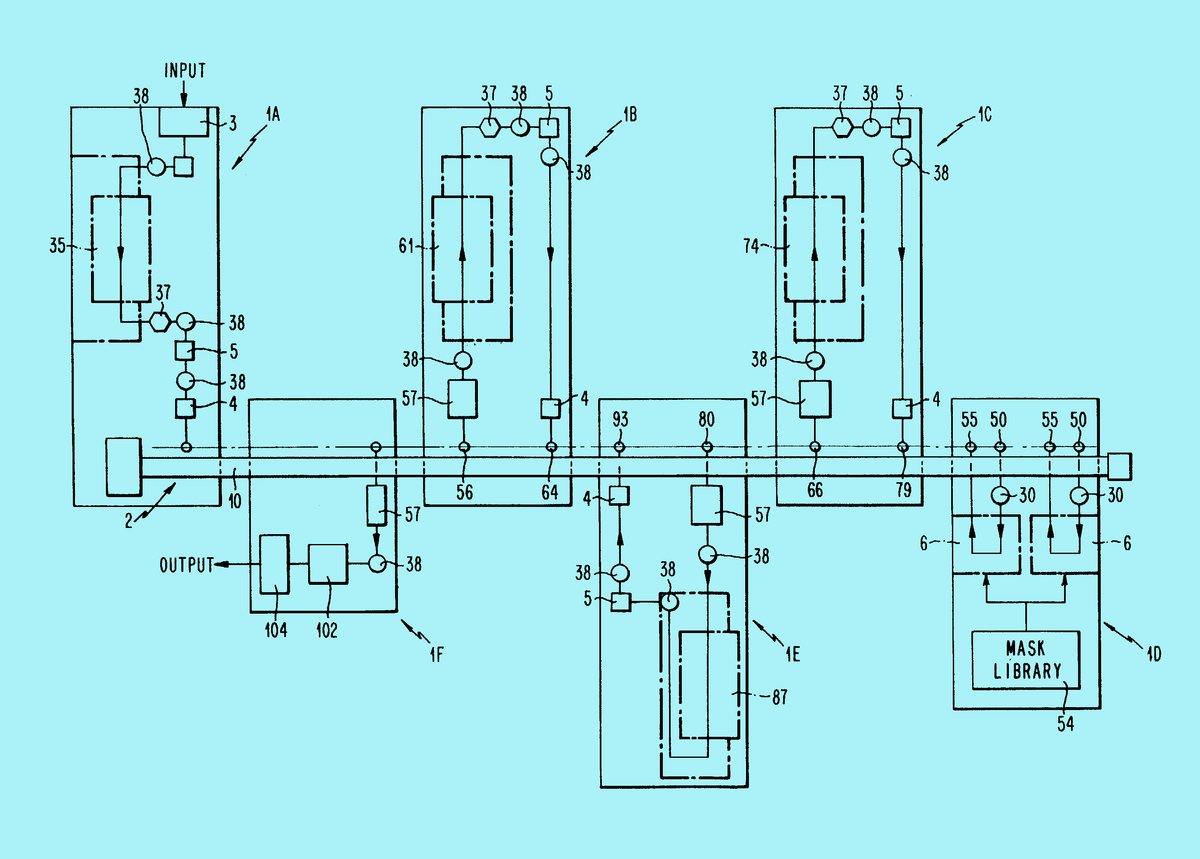
Harding’s team built a dedicated line called Project SWIFT (Semiconductor Wafer Integrated Factory Technology, though Harding insisted it was not an acronym). The line was divided into five sectors, each an automobile‑size enclosure that performed every process step between two lithographic exposures. A monorail “taxi” shuttled a single wafer from sector to sector and back to the same stepper for each mask exposure, guaranteeing perfect alignment.
Architecture
Sector design – Each sector housed wet‑chemistry modules, furnaces, photoresist spin coaters and a pickup port for the taxi. The enclosures maintained clean‑room conditions locally, reducing particle contamination.
Control hierarchy – The top level was an IBM 1800 computer that coordinated the line, recorded wafer IDs, and logged process parameters. Each sector had its own controller; four were custom designs, and one was an IBM System/7, added to showcase IBM’s own factory‑automation computer.
Wafer handling – Most moves used Bernoulli air‑lift handlers that floated the wafer on a cushion of air, avoiding any mechanical contact. The only exception was a forced‑use of an “air‑track” puck system from IBM’s Burlington site, which proved less reliable but was kept to preserve internal politics.
Process flow – A RAM‑II memory chip required four lithographic steps. By routing the wafer back to the same stepper for each exposure, the line avoided cumulative alignment errors. The raw processing time—time the wafer spent actively being worked on—was cut from 48 hours to under 15 hours.
Key innovations that survived
| Innovation | SWIFT implementation | Modern fab equivalent |
|---|---|---|
| Single‑wafer, one‑at‑a‑time processing | One wafer moved through the line while others waited in buffers | Most leading fabs now run single‑wafer tracks for high‑mix, low‑volume lots |
| Centralized computer control | IBM 1800 + sector controllers tracked every wafer | MES/SCADA systems with real‑time data collection |
| Air‑lift wafer handling | Bernoulli handlers lifted wafers without contact | Air‑track and vacuum‑clamp handlers in today’s tools |
| Fixed‑speed spin coaters | Synchronous 3 600 rpm motors eliminated speed controllers | Direct‑drive spin coaters with precise, repeatable speeds |
| Real‑time in‑situ process monitoring | Instrumentation department developed on‑line sensors | Advanced metrology (e.g., scatterometry, ellipsometry) |
Results: a day‑long fab
After three years of design, construction and debugging, the line began production in 1973. Over a series of five runs (mid‑1974 to early‑1975) it achieved:
- Throughput – 58 wafers per day (83 % of design capacity)
- Turn‑around – ~20 hours from bare wafer to testable RAM‑II chips
- Raw process time – 14 hours, a factor of three faster than IBM’s conventional line
- Yield – Equal to the best batch‑processed yield at East Fishkill
- Output – 600 product‑quality wafers containing 17 000 memory chips
The line operated continuously for 12 days during its longest run, proving that a fully automated, single‑wafer fab could meet production targets.
Why the story faded
When IBM cancelled the follow‑on “Future System” computer in 1975, the larger Future Manufacturing System (FMS) line that would have inherited SWIFT’s technology was shelved. Parts of the equipment were repurposed for the QTAT (Quick Turn‑Around Time) line, a later showcase that received more public attention. Consequently, Project SWIFT slipped into obscurity even though its concepts became the backbone of modern semiconductor manufacturing.
Legacy in today’s fabs
Visiting a contemporary fab, you will see many of SWIFT’s ideas in action:
- Automation – Robots and conveyors move wafers between tools without human touch.
- Computer‑driven control – Real‑time monitoring and recipe management are standard.
- Air‑lift handlers – Bernoulli principles keep wafers clean and undamaged.
- Single‑wafer tracks – High‑mix production runs rely on the same “one‑at‑a‑time” philosophy.
- Stepper lithography – Modern extreme‑ultraviolet (EUV) steppers are descendants of the 10:1 reduction stepper used in SWIFT.
Harding’s vision proved that speed, consistency and cleanliness could be engineered together, setting a template that the industry still follows.
Takeaway
Project SWIFT was not a flash‑in‑the‑pan experiment; it was a disciplined engineering effort that reshaped how chips are made. By insisting on a single‑wafer, fully automated line, IBM forced the industry to confront the inefficiencies of batch processing. The result is the highly automated, data‑rich fabs that power today’s electronics. While the name SWIFT may have been lost to history, its DNA runs through every modern semiconductor plant.
For more on the original article, see the IEEE Spectrum feature “The Forgotten Story of How IBM Invented the Automated Fab.”
Comments
Please log in or register to join the discussion