AMD’s sixth‑generation EPYC processor, codenamed Venice, has entered production on TSMC’s N2 (2 nm‑class) process. The 256‑core Zen 6 part promises up to a 70 % uplift over the current EPYC Turin lineup, new SP7 socket support, 1.6 TB/s memory bandwidth and likely PCIe 6.0. With Intel’s next‑gen Xeon delayed, Venice could extend AMD’s server‑CPU market lead while the company also announces a follow‑on Verano SKU and a future Arizona fab ramp.
AMD announces production ramp of EPYC Venice on TSMC’s N2 node
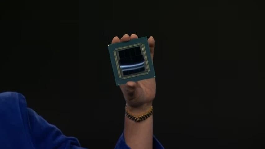
AMD confirmed that its 6th‑gen EPYC processor, code‑named Venice, has moved from engineering samples to full‑scale production on TSMC’s N2 (2 nm‑class) process in Taiwan. The chip integrates up to 256 Zen 6 cores and is positioned as the first high‑performance computing (HPC) product to ship on a 2 nm node.

Technical specifications and claimed performance gains
| Metric | AMD claim | Comparison |
|---|---|---|
| Core count | 256 Zen 6 cores | 2× the maximum core count of EPYC Turin (128 cores) |
| Process node | TSMC N2 (2 nm) | First server‑grade silicon on a 2 nm class node |
| Compute performance | +70 % over EPYC Turin (per‑core) | Roughly the same uplift Intel expects from its next Xeon micro‑architecture, but with a full‑year head start |
| Socket | SP7 (new) | Replaces SP5 used by EPYC Turin |
| Memory subsystem | Up to 16 DDR5 channels, 1.6 TB/s per socket | 2× the bandwidth of the current EPYC Turin platform (≈0.8 TB/s) |
| CPU‑to‑GPU bandwidth | Doubled vs. Turin | Implies native PCIe 6.0 support |
| Power envelope | 400 W – 560 W (configurable) | Similar to top‑end Turin parts, but with higher performance per watt |
AMD’s press release highlights a 70 % compute performance gain measured on a mix of AI inference, HPC Linpack and single‑thread workloads. The claim rests on two factors: the density advantage of N2 (approximately 30 % more transistors per mm² than the 3 nm class) and architectural refinements in Zen 6, including a larger reorder buffer, deeper branch predictor and a new micro‑op cache.
Memory and I/O upgrades
The SP7 socket introduces 16 DDR5 memory channels, delivering a theoretical 1.6 TB/s per‑socket bandwidth. This is a direct response to the growing data‑movement demands of large language models, where memory bandwidth often becomes the bottleneck. In addition, the doubled CPU‑to‑GPU link bandwidth suggests that Venice will ship with PCIe 6.0 (32 GT/s per lane) and possibly CCIX/Compute Express Link extensions, enabling tighter CPU‑GPU coupling for AI accelerators.
Market implications and supply‑chain context
Timing advantage over Intel
Intel’s next‑gen Xeon roadmap has been fluid. The Diamond Rapids (Xeon 7) family, which would directly compete with Venice on core count and single‑thread performance, is rumored to slip to mid‑2027. Intel’s only server product slated for 2026 is Clearwater Forest, an E‑core‑centric design on the 18A process, optimized for density rather than raw performance. With Venice slated for commercial shipments later in 2026, AMD gains a full year of head‑to‑head positioning in the high‑performance segment.
Share‑gain potential
According to Mercury Research, AMD already commands 46 % of server‑CPU revenue in Q1 2026, up from roughly 40 % a year earlier. If Venice delivers the promised performance uplift while keeping the price‑per‑core competitive, AMD could push its share toward the 50 % mark, especially in hyperscale data centers that prioritize AI training throughput.
Production geography and capacity constraints
TSMC began volume production on N2 in late 2023 and is expanding five new 2 nm fabs in 2026 to meet “record demand.” Apple has absorbed the bulk of early N2 capacity for its consumer silicon, leaving limited headroom for server‑grade dies, which have larger footprints and stricter yield requirements. AMD’s decision to also ramp Venice at TSMC’s Arizona Fab 21 Phase 3 signals a diversification strategy, but that facility is not expected to ship volume parts before 2028. Consequently, the initial Venice supply will be Taiwan‑centric, potentially exposing AMD to geopolitical supply‑chain risks.
The Verano follow‑on
AMD also unveiled Verano, another 6th‑gen EPYC SKU built on the same N2 node but tuned for performance‑per‑dollar‑per‑watt. While Venice targets the absolute‑performance tier (large‑scale AI and HPC workloads), Verano will likely occupy the mid‑range cloud segment, where cost efficiency drives purchasing decisions. The dual‑track approach gives AMD flexibility to address both high‑end and price‑sensitive customers without cannibalizing the same silicon pool.
Outlook
If AMD’s 70 % performance claim holds across a representative suite of AI and HPC benchmarks, Venice could become the reference platform for next‑generation large language model training clusters. The combination of 256 cores, 1.6 TB/s memory bandwidth, and PCIe 6.0 creates a compelling package that aligns with the data‑movement‑heavy nature of modern AI workloads.
However, the real test will be yield qualification on the N2 node for a 256‑core server die. Historically, first‑time silicon at a new node experiences a 10‑15 % yield dip before stabilizing, which could constrain early‑volume shipments and give Intel a narrow window to catch up with a delayed Diamond Rapids launch.
In summary, AMD’s Venice marks a decisive step toward 2 nm‑class server silicon, offering a sizable performance jump and a strong defensive position against Intel’s delayed roadmap. The market will watch closely how quickly AMD can translate the announced specifications into real‑world throughput and whether the supply chain can sustain the anticipated demand.
Comments
Please log in or register to join the discussion