Intel confirmed that development on its next‑decade 10‑angstrom (10A) and 7‑angstrom (7A) process technologies is underway, and that the 14A node remains on track for an October PDK release and risk production in 2028. Both new nodes will rely on ASML’s High‑NA EUV platform, extending Intel’s roadmap through the 2030s and shaping the competitive dynamics with TSMC.
Intel Begins Work on 10A and 7A Nodes While 14A PDK Stays on Schedule
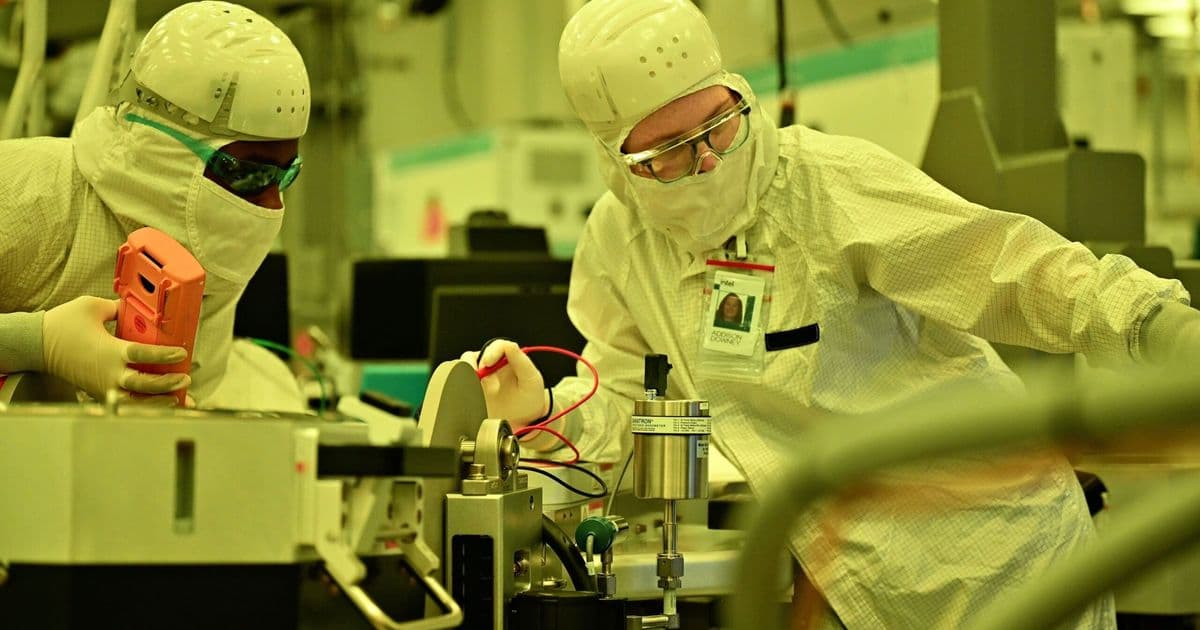
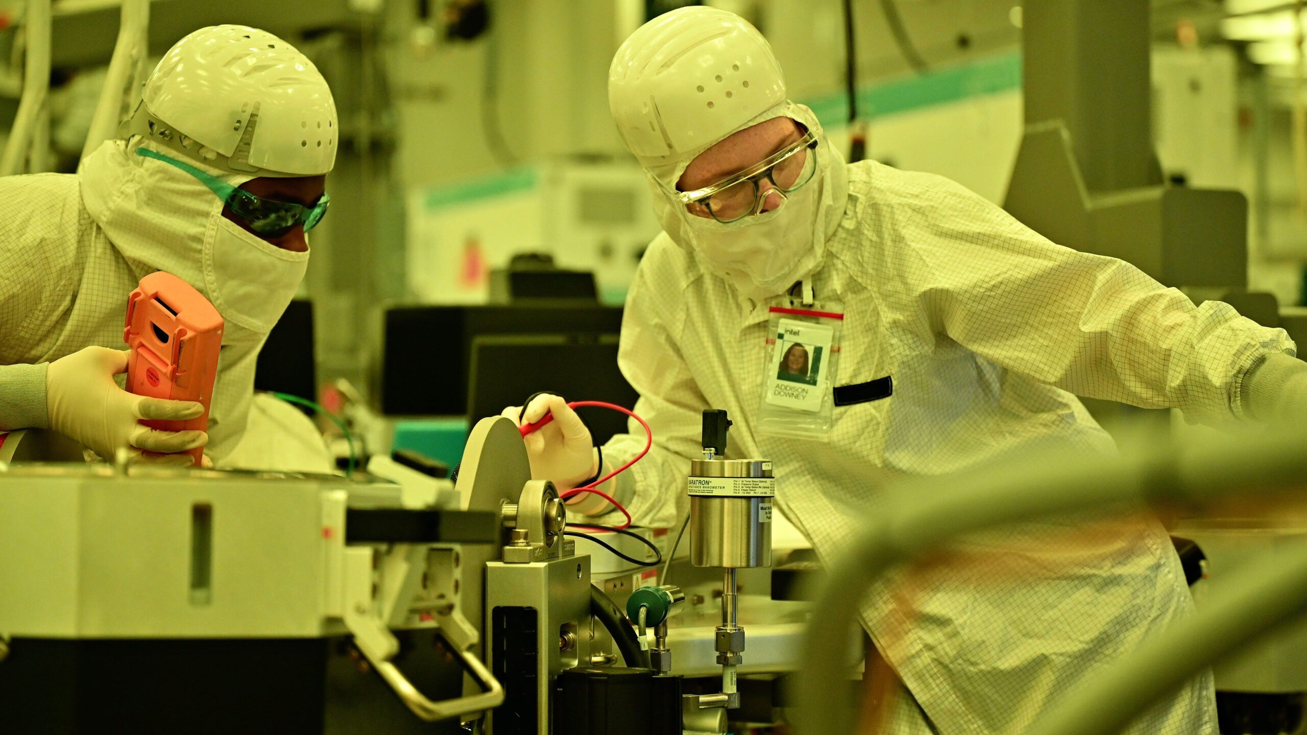 Image credit: Intel
Intel’s CEO Lip‑Bu Tan announced at the JP Morgan Global Technology, Media and Communications Conference that the company has officially started development on its 10‑angstrom (10A) and 7‑angstrom (7A) process technologies. These nodes are slated to follow the current 18A and the upcoming 14A generations, extending Intel’s manufacturing roadmap well into the next decade.
Technical specifications and timeline
| Node | Target pitch (Å) | Expected start of risk production | Expected volume production |
|---|---|---|---|
| 18A | 18 | In production (2024) | 2025‑2026 |
| 14A | 14 | 2028 (risk) | 2029 (volume) |
| 10A | 10 | Early 2030s (concept) | Mid‑2030s |
| 7A | 7 | Late 2030s (concept) | Early 2040s |
14A progress
- PDK version 0.5 released to external customers for test‑chip evaluation.
- PDK version 0.9 targeted for delivery in October 2024, which Intel calls the “Holy Grail” for enabling full‑chip design.
- Risk production scheduled for 2028, with volume production in 2029, aligning roughly with TSMC’s A14 launch.
- High‑NA EUV will be used for select critical layers, making 14A the first Intel node to adopt ASML’s High‑NA scanners in high‑volume manufacturing.
10A and 7A outlook
- Both nodes will leverage High‑NA EUV for the majority of layers, requiring new photoresists, pellicles, and computational lithography flows.
- Intel is collaborating with ASML and a broad ecosystem of mask makers, metrology vendors, and design‑tool providers to mature the full stack before silicon production.
- The roadmap emphasizes long‑term visibility for customers; Intel plans to publish detailed node‑level forecasts well in advance of tape‑out, a practice that helps partners secure capacity and co‑development budgets.
Market implications
Competitive positioning against TSMC
- Node comparison – TSMC’s A14 (≈14 Å) will be in high‑volume production by late 2028, but it targets a broader market that includes mobile and consumer chips. Intel’s 14A is engineered for data‑center workloads, featuring backside power delivery (BPD) and higher transistor density optimized for server‑grade CPUs and accelerators.
- Yield trajectory – TSMC typically reaches >80 % yield within the first few months of HVM, while Intel historically ramps yields more gradually, especially when introducing new lithography equipment. The High‑NA transition adds complexity: new mask sets, new pellicles, and tighter overlay budgets could extend Intel’s yield‑learning curve.
- Capacity strategy – Intel will run early 14A volume at its development fabs (e.g., D1X, D2X) before scaling to larger capacity lines. This phased approach may limit initial output but gives Intel control over process refinement.
Supply‑chain considerations
- The High‑NA EUV ecosystem is still nascent. ASML expects the first test chips on High‑NA tools within months, but full‑scale fab integration will require new resist chemistries and metrology solutions. Intel’s early engagement with partners reduces the risk of bottlenecks in mask and pellicle supply.
- PDK availability is a critical enabler for third‑party design houses. By delivering the 0.9 PDK in October, Intel gives customers a full design flow roughly 18 months before risk production, matching the timeline traditionally seen at TSMC.
- Capacity planning for 14A will hinge on demand from a handful of large customers (likely hyperscalers and enterprise‑class silicon vendors). Intel’s statement that “multiple customers are engaged” suggests a growing order book, but the lack of disclosed names leaves the market uncertain about the node’s immediate revenue impact.
Long‑term outlook
- The announcement of 10A and 7A signals Intel’s commitment to maintain a multi‑node roadmap that can support emerging workloads such as AI inference, high‑performance computing, and next‑generation networking.
- By aligning all three upcoming nodes (14A, 10A, 7A) around High‑NA EUV, Intel aims to standardize the lithography platform, potentially reducing per‑node transition costs and shortening development cycles for future generations.
- If Intel can achieve competitive yields on 14A, the company will be positioned to capture a larger share of the high‑performance server market, where customers value the combination of BPD, high core counts, and Intel’s integrated memory‑fabric architecture.
Bottom line
Intel’s roadmap now stretches from the imminent 14A node, with a PDK slated for October 2024, to speculative 10A and 7A processes that will rely on High‑NA EUV. The success of 14A will set the tone for Intel’s ability to compete with TSMC’s A14 and later nodes, especially in the data‑center segment where performance and power delivery are paramount. Early PDK releases, transparent roadmaps, and deep ecosystem collaboration are Intel’s primary tools for mitigating the supply‑chain risks inherent in the High‑NA transition.
For further reading on High‑NA EUV and Intel’s foundry strategy, see the ASML High‑NA overview and Intel’s process technology page.
Comments
Please log in or register to join the discussion