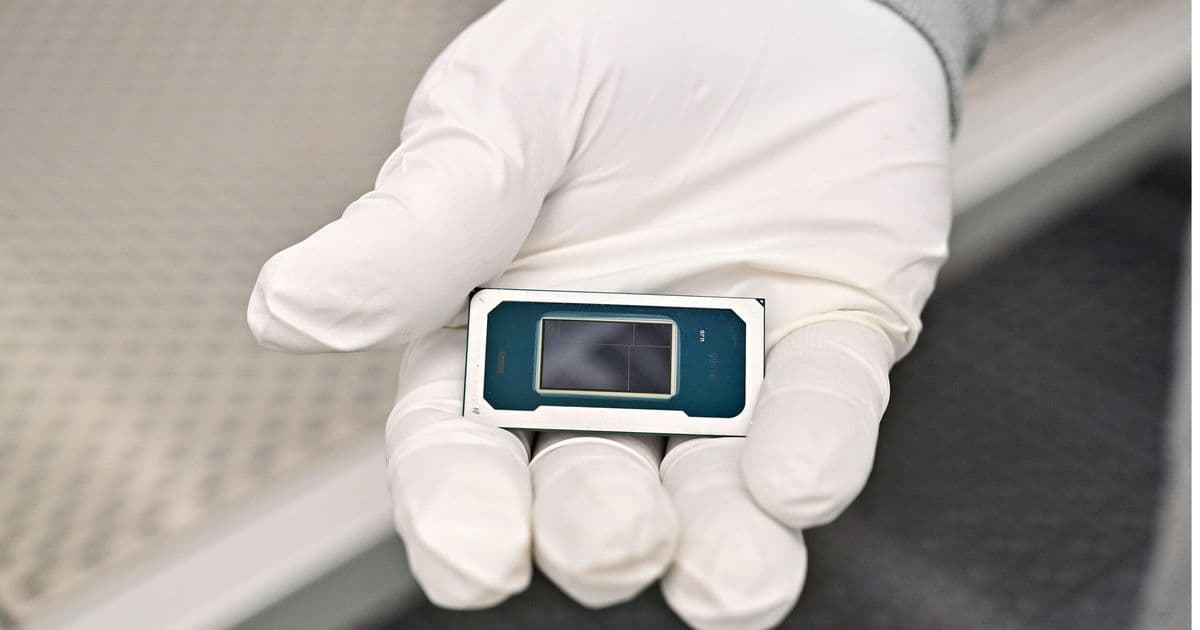
Intel's Core Ultra 300-series Panther Lake-H processors finally show their die shots, revealing a three-tile design with 18A compute tile, Xe3 GPU, and I/O components.
Intel has finally revealed the die shots of its Core Ultra 300-series Panther Lake-H processors, offering a detailed look at the three-tile architecture that powers the company's latest high-performance mobile chips. The images, published by Kurnal-Insights.com, show the intricate layout of the 18A process technology compute tile, Xe3 graphics tile, and I/O tile that make up these processors.
18A Compute Tile Architecture
The compute tile, or system-on-chip tile as Kurnal refers to it, represents Intel's most advanced manufacturing achievement to date. Built on the company's 18A process technology, the tile integrates a sophisticated core configuration designed for both performance and efficiency.
At the heart of the compute tile are four high-performance Cougar Cove cores with 3 MB L2 cache, capable of running at up to 5.1 GHz. These are complemented by eight space-efficient Darkmont cores operating at up to 3.8 GHz, and four low-power Darkmont cores running at up to 3.7 GHz. This heterogeneous architecture allows the processor to dynamically allocate workloads to the most appropriate core type based on performance requirements and power constraints.
Interestingly, the die shot reveals no physical differences between the Darkmont E-core cluster with 4 MB L2 cache and the Darkmont LPE-core cluster with 4 MB L2 cache. However, the 18 MB L3 cache is strategically split into three slices positioned close to the P-core and E-core clusters, while being located far from the LPE cluster. This placement suggests Intel prioritized cache proximity for the performance-oriented cores.
The die also shows three slices of Neural Processing Units (NPUs), each with their own 4.5 MB of cache. This slicing approach serves a dual purpose: it enables Intel to disable defective slices without scrapping the entire die, and it provides flexibility in configuring different performance tiers. If a slice contains defects, it can be disabled, allowing the chip to be sold at a lower tier while still maintaining functionality.
Memory Side Cache Innovation
One of the most intriguing features revealed in the die shot is the 128-bit DDR5/LPDDR5X-9600 memory controller's 8MB memory side cache (MSC). This cache structure is designed to buffer memory traffic and reduce latency and bandwidth pressure when multiple cores or execution units simultaneously access RAM.
While Panther Lake is not Intel's first use of a memory-side cache-type structure, the implementation differs significantly from earlier concepts like the CrystalWell L4 cache. The purpose and architecture have evolved considerably over time. It's worth noting that Intel's MSC should not be directly compared to Apple's system-level cache, which acts as the last level cache for the entire system-on-chip. Intel's approach is more targeted, focusing on specific memory traffic patterns and core interactions.
Integrated Media and Display Engines
The compute tile also houses integrated media and display engines, a feature that provides Intel with additional flexibility in CPU configurations. This arrangement allows the company to attach various GPUs and I/O dies while maintaining essential functionality within the compute tile itself. This modular approach suggests Intel is positioning itself for greater flexibility in future product configurations and potential market segments.
The overall architecture of the compute tile bears strong resemblance to Intel CPUs released in recent years, which almost certainly indicates the use of a ring bus interconnect. However, the SoC tile also features high-performance interfaces that connect to the GPU and I/O die tiles, suggesting a more complex interconnect fabric than traditional ring architectures.
Xe3 Graphics Tile Details
The graphics tile integrates 12 Intel Xe3 clusters and 16MB of L2 cache implemented across eight tiles. This tiled approach to cache implementation, similar to the compute tile's strategy, allows Intel to disable faulty GPU clusters or cache tiles to improve yield of sellable chips. Graphics processing units are notoriously difficult to manufacture without defects due to their massive transistor counts and complex architectures, so this binning strategy is crucial for achieving acceptable manufacturing yields.
I/O Tile Complexity
The I/O tile proves to be just as interesting as the compute tile, carrying a Thunderbolt 5 controller along with two TB 5.0 PHYs that occupy a significant portion of the die. The tile also includes a Wi-Fi/Bluetooth controller with appropriate physical interfaces, PCIe 5.0 x4 PHY, two PCIe 4.0 x4 PHYs, and USB PHYs.
Unlike the compute and graphics tiles, the I/O tile appears to be the most critical component for die viability. If defects occur in the I/O tile, it likely means the entire die must be scrapped, as the I/O functionality is essential for the processor to function in any capacity. This makes the I/O tile a potential yield bottleneck in the manufacturing process.
Manufacturing and Yield Implications
The three-tile architecture represents Intel's strategy for managing the complexities of advanced semiconductor manufacturing. By splitting the processor into distinct functional tiles, Intel can optimize each component for its specific requirements while providing flexibility in how defective areas are handled.
The compute tile's 18A process technology represents Intel's most advanced manufacturing capability, while the graphics and I/O tiles likely use more mature process nodes better suited to their specific requirements. This heterogeneous manufacturing approach allows Intel to balance cutting-edge performance with manufacturing practicality.
Market Position and Competition
The Panther Lake-H architecture positions Intel competitively in the high-performance mobile processor market. The combination of high-performance cores, efficient cores, and low-power cores mirrors strategies employed by competitors but with Intel's unique implementation details.
The integration of advanced features like the memory side cache and the sophisticated NPU implementation suggests Intel is targeting not just traditional computing workloads but also AI and machine learning applications that are becoming increasingly important in mobile computing scenarios.
Technical Specifications Summary
- Compute Tile: 18A process technology
- Core Configuration: 4x Cougar Cove (up to 5.1 GHz), 8x Darkmont (up to 3.8 GHz), 4x Darkmont LPE (up to 3.7 GHz)
- Cache: 18 MB L3 (3 slices), 4.5 MB NPU cache per slice, 8 MB memory side cache
- Graphics Tile: 12x Xe3 clusters, 16 MB L2 cache (8 tiles)
- I/O Tile: Thunderbolt 5 controller, PCIe 5.0 x4, PCIe 4.0 x4 (2), Wi-Fi/Bluetooth, USB PHYs
These die shots provide valuable insight into Intel's architectural direction and manufacturing strategies as the company works to regain its competitive position in the processor market. The three-tile approach, advanced process technology, and sophisticated feature integration demonstrate Intel's commitment to innovation despite the challenges of advanced semiconductor manufacturing.
The images also highlight the increasing complexity of modern processor design, where different functional blocks must be carefully balanced and optimized for both performance and manufacturability. As Intel continues to refine its process technology and architectural approaches, the lessons learned from Panther Lake-H will likely influence future processor designs across the company's product portfolio.
Comments
Please log in or register to join the discussion