The Tokyo Metropolitan Art Museum has created unique bookmarks using actual PCB manufacturing techniques to form miniature Tokyo Metro maps, selling out quickly at $15 each.
The Tokyo Metropolitan Art Museum has introduced a fascinating intersection of electronics manufacturing and art with its new line of PCB-style bookmarks, featuring miniature Tokyo Metro maps created using genuine printed circuit board fabrication techniques.
(Image credit: The Tokyo Metropolitan Art Museum)
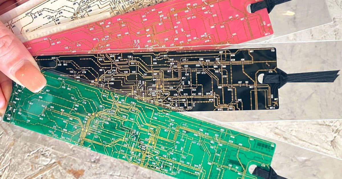
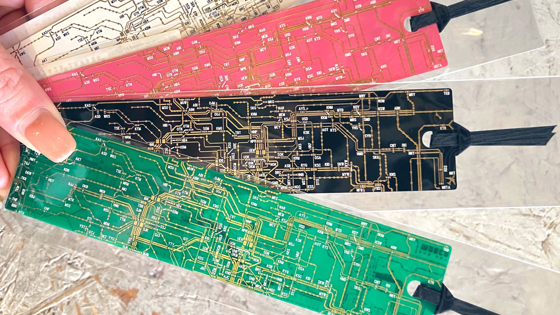
These bookmarks, priced at approximately $15 each, come in four color variations - red, white, green, and black - and immediately sold out upon release. The museum's online store announced the product on January 25, 2026, with the Japanese text noting that "actual circuit boards with a thickness of 0.3mm" were used in their creation.
What makes these bookmarks particularly remarkable is the level of authenticity in their production. According to the museum, "The materials, processes, and manufacturing methods are exactly the same as those used for real circuit boards." This means the bookmarks underwent the same PCB fabrication process as actual electronic components, including copper etching and surface finishing.
(Image credit: The Tokyo Metropolitan Art Museum)
The design process itself demonstrates an unusual blend of artistic vision and technical expertise. The museum's webstore explains that the bookmarks were created using "PCB-specific CAD software," suggesting that either a fine artist learned electronics design tools or the museum collaborated with someone possessing both artistic and engineering skills. Each trace was "drawn by hand with a mouse," resulting in a meticulously crafted piece that blends electronic engineering with art.
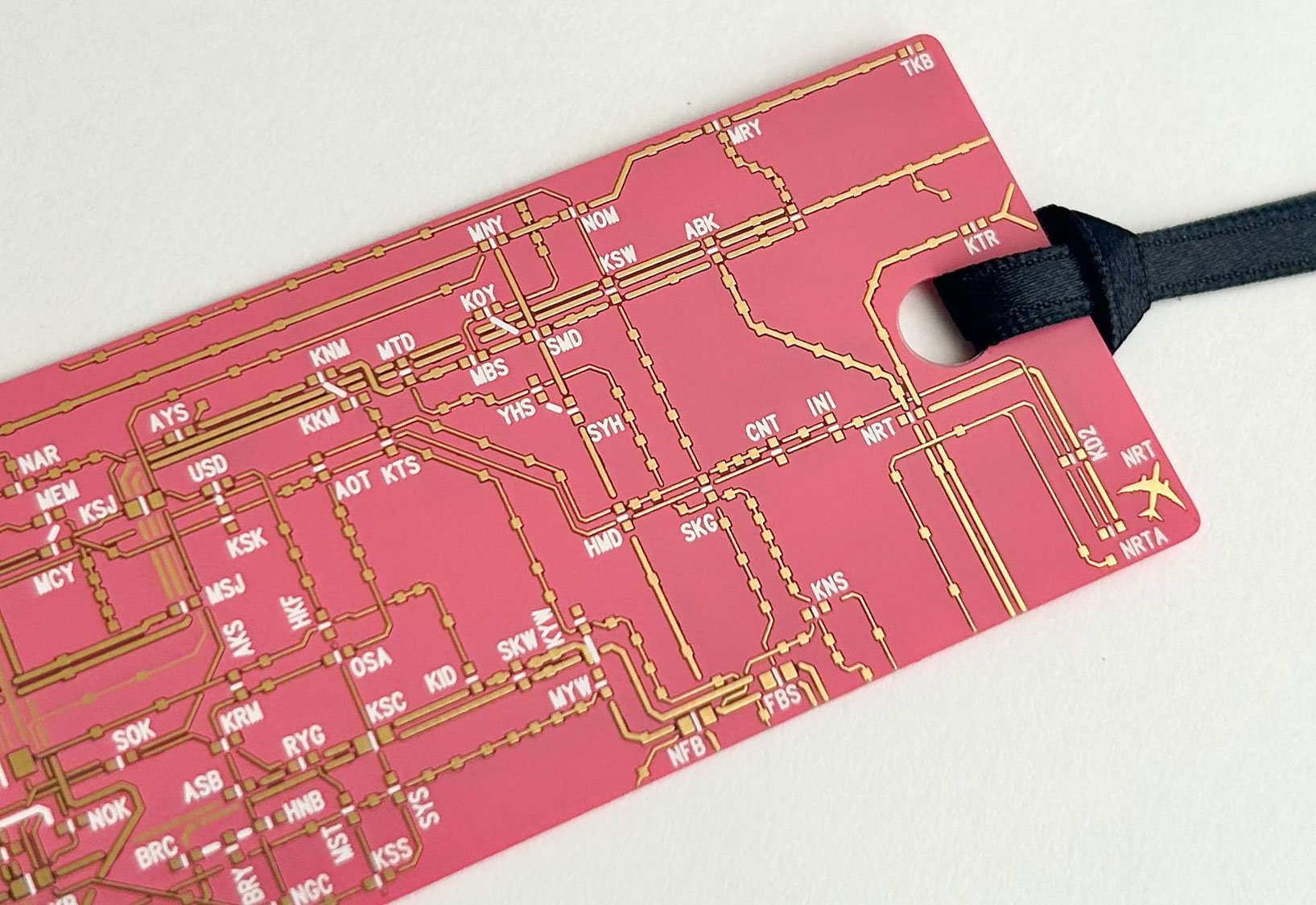
Upon closer inspection, the copper traces form an accurate representation of the Tokyo Metro system, stretching from Ofuna Station in the west to Narita Airport in the east. This transforms what appears to be random electronic circuitry into a functional transit map, creating a clever optical illusion that rewards careful observation.
(Image credit: The Tokyo Metropolitan Art Museum)
Safety considerations were clearly taken into account during production. Unlike real populated PCBs that could damage book pages with their through-hole component spikes and variable surface components, these bookmarks have been carefully modified. The museum notes that "0.15mm of copper foil has been removed from the board's edges" to prevent damage to books, planners, or hands. Additionally, close inspection reveals that while the traces are authentic, no actual electronic components are mounted on the boards.
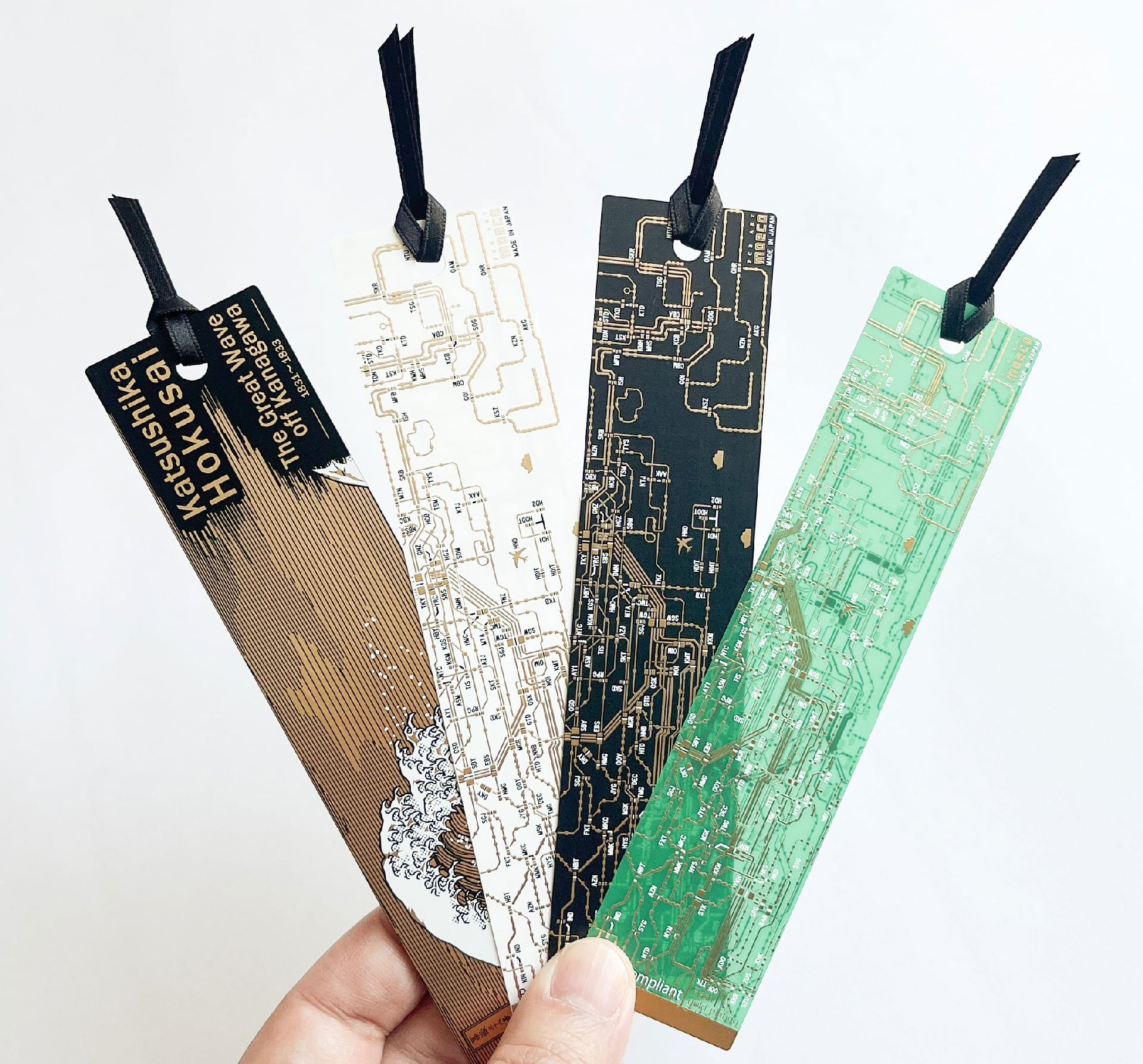
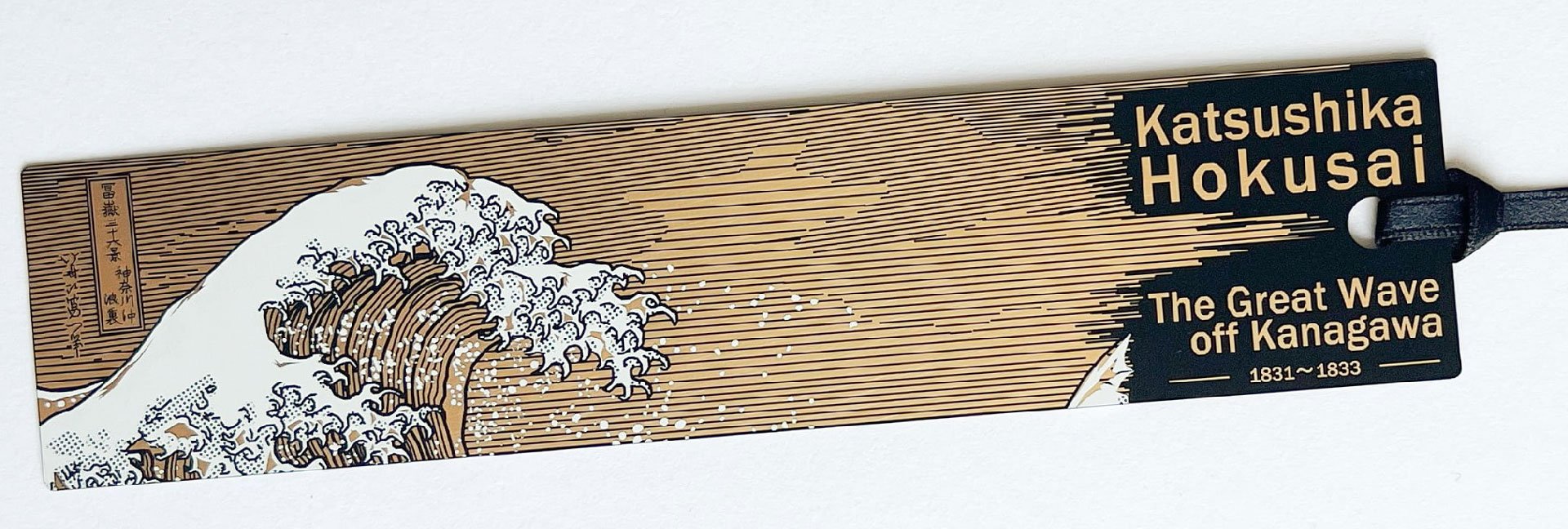
The bookmarks measure 140 x 32 x 0.45mm (approximately 6 inches by 1.25 inches by 0.018 inches), making them slim enough to function as practical bookmarks while maintaining the authentic feel of a circuit board. The museum has also created other designs, including a PCB representation of Hokusai's famous "The Great Wave off Kanagawa," though this variant has also sold out.
(Image credit: The Tokyo Metropolitan Art Museum)
The rapid sell-out demonstrates strong consumer interest in this unique fusion of technology and art. The museum has indicated plans to restock, suggesting that these PCB bookmarks may become a recurring souvenir item. This product represents an innovative approach to museum merchandise, transforming the typically utilitarian world of electronics manufacturing into collectible art objects that celebrate both Tokyo's transit system and the aesthetic beauty of circuit board design.
The success of these bookmarks raises interesting questions about the future of tech-inspired art and whether other museums might explore similar approaches using authentic manufacturing processes from various industries. For now, electronics enthusiasts and art collectors alike are eagerly awaiting the museum's restock announcement.
Comments
Please log in or register to join the discussion