On May 11, 1951 MIT engineer Jay Forrester filed the patent that defined coincident‑current magnetic core memory, a technology that powered mainframes for two decades and shaped early computer supply chains. This article reviews the core’s physical design, performance metrics, and the legal‑supply‑chain battles that followed.
75‑Year Milestone for Magnetic Core Memory
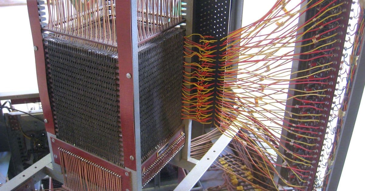
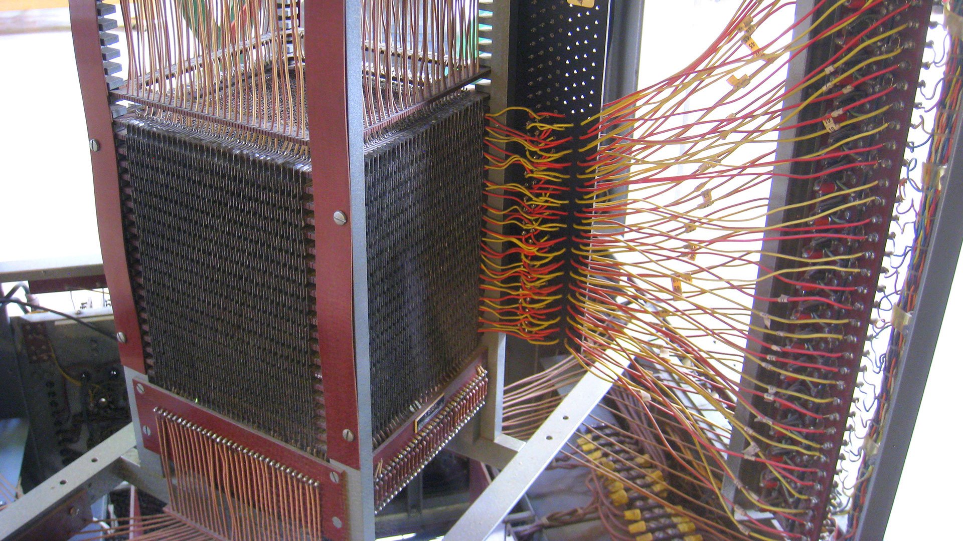
On May 11, 1951 Jay Forrester submitted a patent application for coincident‑current magnetic core memory (U.S. Patent 2736880, granted February 1956). The filing marked the start of a storage technology that would dominate mainframe computers from the mid‑1950s through the early‑1970s.
Technical specifications of the original core bank
| Parameter | Original implementation | Modern comparison |
|---|---|---|
| Core material | Ferrite ring, ~2 mm diameter | Ferrite still used in niche RF components |
| Bit size | 1 bit per core (magnetized clockwise = 1, counter‑clockwise = 0) | 1 bit per cell in SRAM, 1 bit per transistor in DRAM |
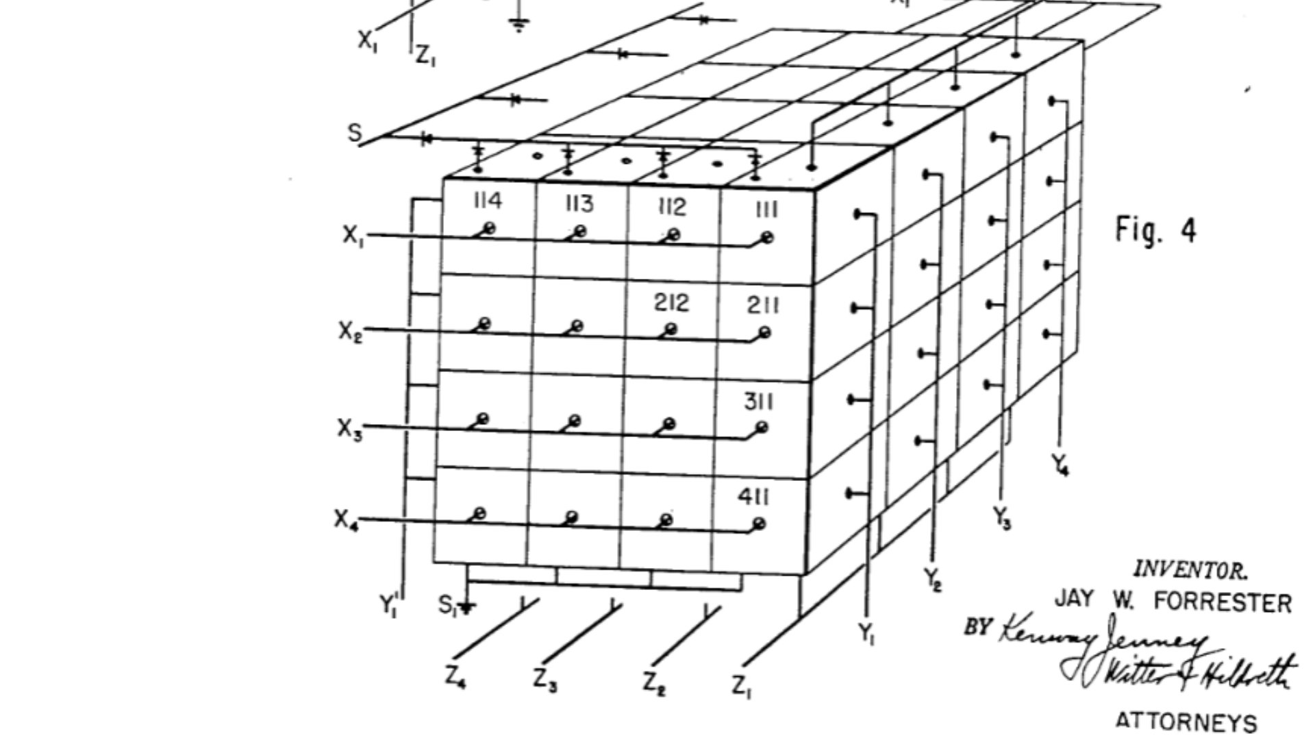
| Access method | Coincident‑current: two perpendicular wires (X and Y) carry half‑current; only the intersecting core sees full current | Row/column address lines in DRAM, but with voltage‑level sensing instead of magnetic polarity |
| Access time | 1–2 µs (typical for Whirlwind) | 10–20 ns for modern DDR4 DRAM |
| Density | ~2 Kb per bank (≈2 000 cores) | >64 Gb per DRAM chip (≈8 000 × 8 Mbits) |
| Power consumption | Tens of milliwatts per bank (static power negligible) | Milliwatts per GB for DDR4, but static leakage dominates in SRAM |
The core memory’s three‑dimensional addressing allowed a relatively small wire count to reach millions of bits. For example, a 64 K‑core bank used only 256 X‑lines and 256 Y‑lines, a 2‑log‑2 reduction compared with a naïve one‑wire‑per‑bit layout.
Why the technology mattered for supply chains
- Component standardization – Ferrite cores were produced by a handful of magnetic‑material firms (e.g., Ferranti, Raytheon). Their dimensions and magnetic properties were tightly specified, enabling multiple computer manufacturers to source identical parts.
- Manufacturing yield – Core winding was a manual process, but the low defect rate (≈0.1 % per core) meant that a 2 Kb bank could be assembled with acceptable scrap levels. The predictable yield kept bill‑of‑materials costs stable across IBM, UNIVAC, and Honeywell lines.
- Repairability – Faulty cores could be replaced by hand with a soldering iron, a feature that extended system uptime for defense installations such as SAGE. This serviceability reduced total cost of ownership for government contracts.
These supply‑chain characteristics helped the technology spread quickly despite the labor‑intensive assembly.
Legal battles and their impact on the market
- Jan Rajchman (RCA) filed a similar claim eight months before Forrester. RCA’s early filing forced MIT to produce exhaustive evidence—purchase orders, telephone logs, lab notebooks—to prove priority.
- An Wang (Harvard) patented a different core‑addressing scheme, which IBM bought in 1955 for $500 000. The acquisition gave IBM a foothold in the emerging market and accelerated its own core‑memory product line.
- IBM vs. MIT – IBM challenged the breadth of Forrester’s patent for years. The dispute settled in 1964 with a $13 million payment, the largest patent settlement at the time. The settlement cleared the way for IBM to mass‑produce core memory without fear of infringement litigation, stabilizing the supply chain for the next decade.
These legal outcomes directly influenced component sourcing. After the settlement, core manufacturers could negotiate bulk contracts with IBM, leading to economies of scale that lowered per‑core cost from roughly $0.10 in 1958 to under $0.01 by 1965.
From core memory to modern semiconductor RAM
The magnetic core’s principle—non‑volatile storage of a binary state—prefigured later semiconductor RAM designs. DRAM’s charge‑storage cell mirrors the core’s binary magnetization, but replaces magnetic hysteresis with capacitor leakage. SRAM’s latch architecture, while faster, still relies on the same two‑state logic.
Key performance gaps illustrate the evolution:
- Latency dropped from microseconds to nanoseconds, a factor of >1 000.
- Density increased from kilobits per board to gigabits per die, a factor of >1 000 000.
- Power shifted from static magnetic bias (tens of milliwatts per bank) to dynamic charge‑pump leakage (millwatts per gigabyte), enabling mobile devices.
Despite these advances, core memory’s durability and radiation hardness keep it relevant for aerospace and nuclear‑facility control systems, where modern DRAM would fail.
Legacy and concluding perspective
Jay Forrester’s 1951 filing did more than introduce a new storage cell; it established a supply‑chain model where a limited set of specialized components supported a rapidly expanding computer market. The subsequent legal settlements clarified intellectual‑property boundaries, allowing manufacturers to invest in high‑volume production without disruptive litigation.
Seventy‑five years later, the core’s magnetic principles still echo in emerging non‑volatile memories such as MRAM, which use similar ferromagnetic tunnel junctions to store bits. The continuity underscores how a 2 Kb prototype can shape technology trajectories for decades.
For further reading, see the original U.S. Patent 2736880 and the MIT archival collection on Project Whirlwind.
Comments
Please log in or register to join the discussion