A new electron‑beam algorithm lets scientists move columns of individual atoms inside a solid at room temperature, creating tens of thousands of quantum defects in minutes. The technique promises programmable quantum materials for sensors, memory and future quantum computers.
A breakthrough in atomic‑scale engineering
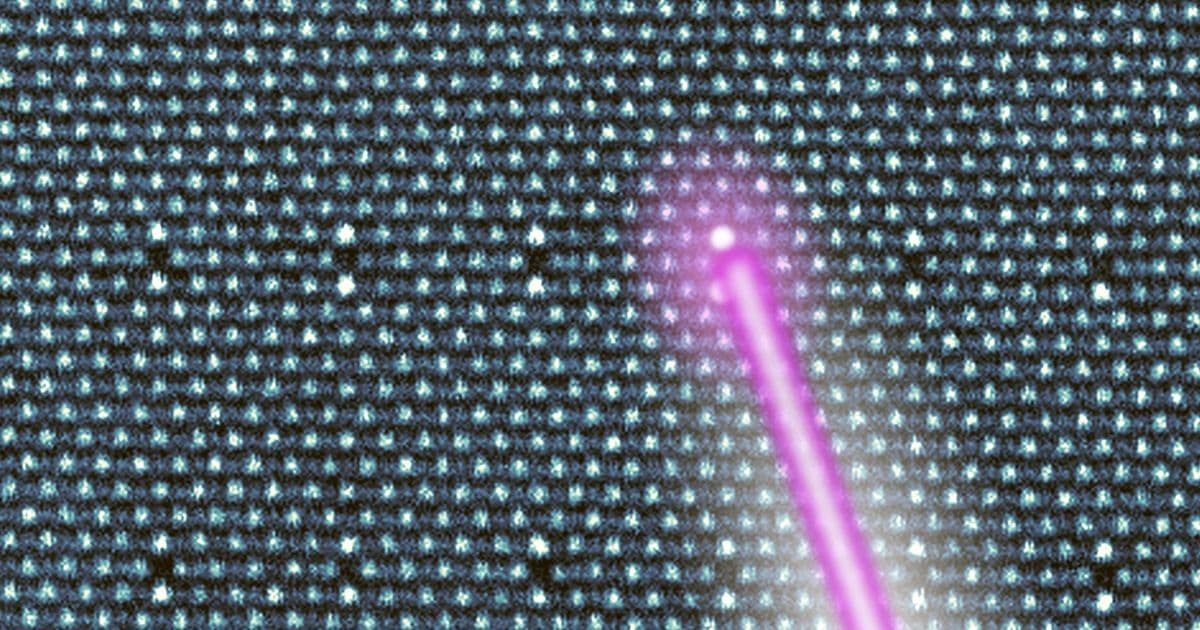
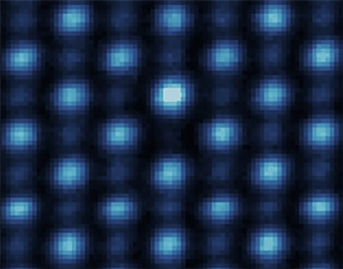
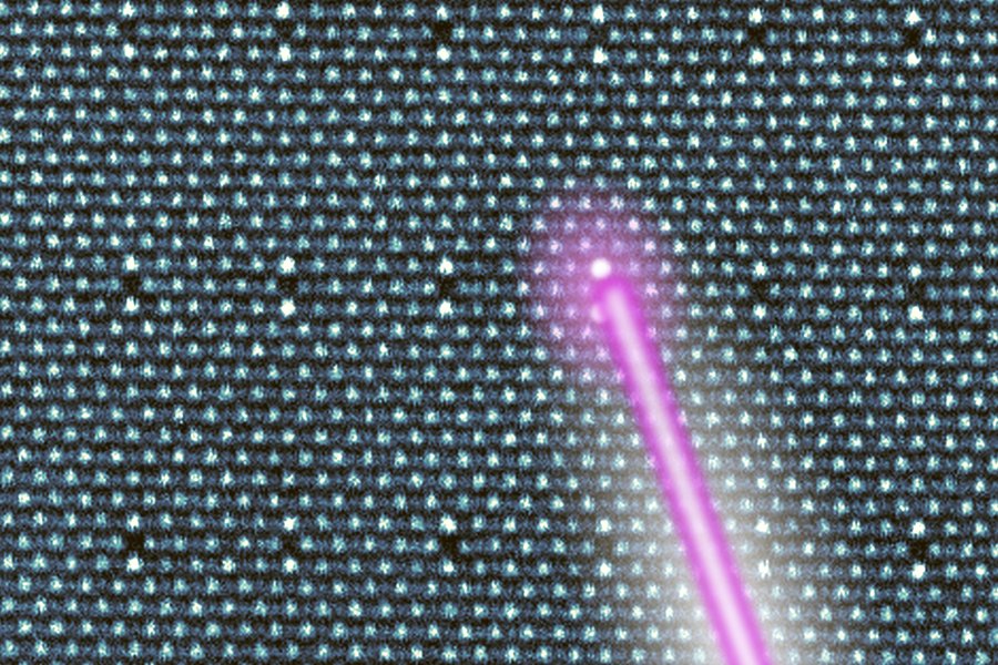
A team spanning MIT, Oak Ridge National Laboratory and several international partners has demonstrated a way to move tens of thousands of atoms inside a crystal lattice in a matter of minutes, all at room temperature. By pairing a high‑resolution electron microscope with a suite of custom algorithms, the researchers can steer an electron beam with picometer precision, nudging columns of atoms along a pre‑designed path. The result is a dense pattern of engineered defects that can endow a material with exotic quantum properties.

How the technique works
- Beam positioning algorithm – The core of the method is a real‑time feedback loop that estimates the beam’s location inside the solid using only a handful of electrons. This minimizes damage while delivering sub‑nanometer accuracy.
- Oscillating scan trajectory – Once the target atom is identified, the beam follows a tight, oscillating loop that pushes an entire column of atoms a few lattice sites forward, much like swiping a finger across a screen.
- Rapid defect generation – By spending roughly one second per site, the system can write more than 40,000 vacancies and interstitials in a 13‑nm‑thick crystal of chromium‑sulphide‑bromide in under an hour.
The approach builds on the legacy of the 1989 IBM scanning‑tunnelling‑microscope demonstration, which arranged 35 atoms on a surface over many hours. Unlike that early work, the new method operates in three dimensions, works at ambient conditions, and scales to orders of magnitude more atoms.
Real‑world applicability
Quantum information processing
The engineered defects act as localized quantum bits (qubits) that can be positioned close enough to interact coherently. By arranging them in specific geometries, researchers can simulate molecular electronic structures or create dense quantum‑memory arrays that remain stable outside ultra‑high‑vacuum chambers.
Sensing and photonics
Defect‑based color centers are already used for magnetic and temperature sensing. A programmable lattice of such centers could yield sensors with tailored spectral responses, enabling on‑chip magnetometers that operate at room temperature.
Magnetic and optical devices
The ability to embed defect columns beneath the surface protects them from oxidation and mechanical wear, opening pathways to robust magnetic memory or nonlinear optical materials whose response is defined by the engineered atomic pattern.
Limitations and next steps
- Material compatibility – The proof‑of‑concept used chromium‑sulphide‑bromide because its bonding makes atoms easy to displace. Extending the method to silicon, diamond or other technologically relevant substrates will require material‑specific algorithm tuning.
- Beam‑induced damage – Although the algorithm minimizes electron exposure, cumulative damage can still alter lattice strain over long writing sessions. Ongoing work focuses on adaptive dose control to keep the crystal’s bulk properties intact.
- Scalability beyond 10⁵ atoms – Moving millions of atoms will demand faster beam steering hardware and parallelization across multiple microscopes. The team is exploring FPGA‑based control loops to shave milliseconds off each step.
Outlook
The MIT‑Oak Ridge collaboration has turned the notion of “programmable matter” from a theoretical curiosity into a practical laboratory tool. By providing a fast, room‑temperature route to sculpt atomic‑scale defects, the technique bridges the gap between single‑atom manipulation and bulk material engineering. As algorithms improve and the method is adapted to a broader class of crystals, we can expect a new generation of quantum devices that are designed atom by atom rather than discovered by trial and error.
The research was published in Nature on May 13, 2026. Funding was provided by the U.S. Department of Energy and the National Science Foundation.
Comments
Please log in or register to join the discussion