MIT scientists have directly characterized the three-dimensional atomic structure of relaxor ferroelectrics for the first time, revealing the source of their unique properties and enabling better design of advanced electronic devices.
For decades, relaxor ferroelectrics have been essential components in technologies ranging from medical ultrasound equipment to sonar systems and microphones. Despite their widespread use, the atomic-level structure responsible for their exceptional properties remained elusive. Now, researchers at MIT and collaborating institutions have successfully mapped the three-dimensional atomic structure of these materials, providing crucial insights that could revolutionize the design of next-generation computing, energy storage, and sensing devices.
The findings, published in Science, reveal a hierarchy of chemical and polar structures that span from atomic to mesoscopic scales. This breakthrough resolves a long-standing mystery in materials science and provides a framework for refining computational models used to engineer advanced materials.
"Now that we have a better understanding of exactly what's going on, we can better predict and engineer the properties we want materials to achieve," says corresponding author James LeBeau, MIT's Kyocera Professor of Materials Science and Engineering. "The research community is still developing methods to engineer these materials, but in order to predict the properties those materials will have, you have to know if your model is right."
Probing the Unseen
Relaxor ferroelectrics are unique materials that exhibit exceptional energy storage and sensing capabilities. Previous simulations suggested that when an electric field is applied, interactions between positively and negatively charged atoms in different nanoregions of these materials contribute to their distinctive properties. However, the details of these nanoregions had been impossible to directly measure until now.
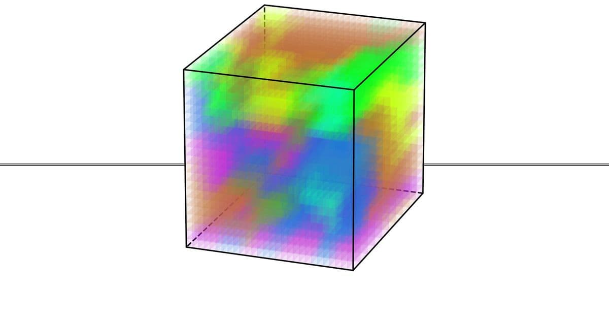
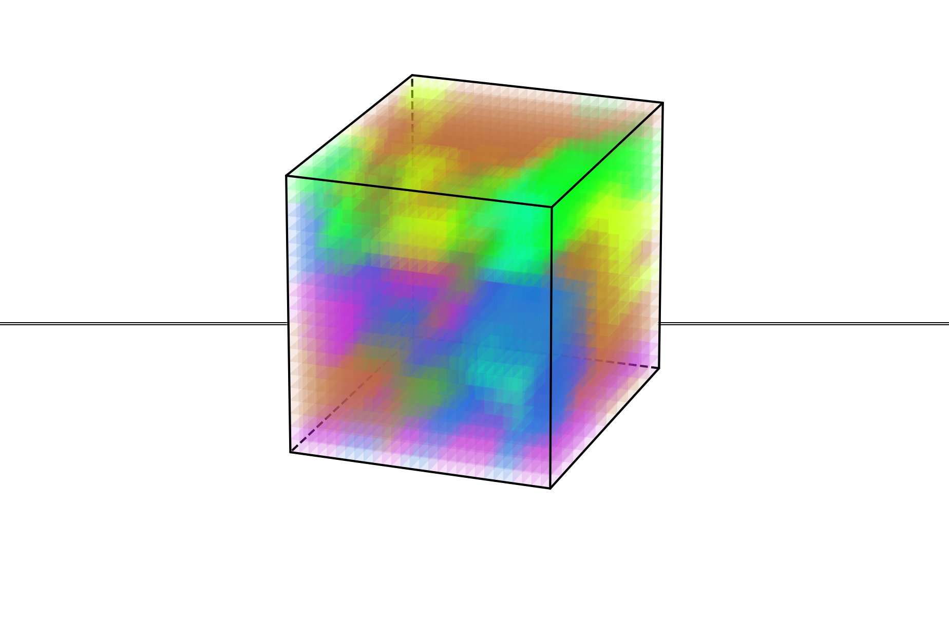
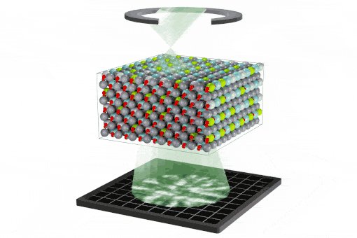
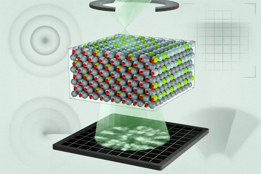
For their research, the team studied a lead magnesium niobate-lead titanate alloy, a relaxor ferroelectric commonly used in sensors, actuators, and defense systems. They employed an emerging measurement technique called multi-slice electron ptychography (MEP), which involves moving a nanoscale-sized probe of high-energy electrons across a material and measuring the resulting electron diffraction patterns.
"We do this in a sequential way, and at each position, we acquire a diffraction pattern," explains Menglin Zhu, co-first author of the paper. "That creates regions of overlap, and that overlap has enough information to use an algorithm to iteratively reconstruct three-dimensional information about the object and the electron wave function."
The technique revealed that many regions of differing polarization in the material were significantly smaller than predicted by leading simulations. This discovery prompted the researchers to reconsider how these materials are modeled and understood.
"We realized the chemical disorder we observed in our experiments was not fully considered previously," says co-first author Michael Xu. "Working with our collaborators, we were able to merge the experimental observations with simulations to refine the models and better predict what we see in experiments."
From Discovery to Application
The research team, which includes scientists from MIT, the University of Alabama at Birmingham, the Korea Advanced Institute of Science and Technology, the University of Pennsylvania, and Rice University, fed their new experimental data back into existing computer simulations and refined the models to better reflect the material's behavior under different conditions.
"Previously, these models basically had random regions of polarization, but they didn't tell you how those regions correlate with each other," Xu notes. "Now we can tell you that information, and we can see how individual chemical species modulate polarization depending on the charge state of atoms."
This breakthrough has significant implications for materials engineering. The electron ptychography technique demonstrated in this study opens new avenues for research into complex, disordered materials that are prevalent in modern technology but challenging to characterize.
"This study is the first time in the electron microscope that we've been able to directly connect the three-dimensional polar structure of relaxor ferroelectrics with molecular dynamics calculations," Xu explains. "It further proves you can get three-dimensional information out of the sample using this technique."
Toward Better Materials
The ability to directly characterize and understand the atomic structure of relaxor ferroelectrics could lead to significant advancements in several technological areas. These materials are crucial for capacitors in energy storage systems, components in medical ultrasound devices, and sensors in various industrial applications.
"Materials science is incorporating more complexity into the material design process — whether that's for metal alloys or semiconductors — as AI has improved and our computational tools have become more advanced," LeBeau says. "But if our models aren't accurate enough and we have no way to validate them, it's garbage in garbage out. This technique helps us understand why the material behaves the way it does and validate our models."
The researchers believe their approach could one day help engineer materials with advanced electronic behaviors for improved memory storage, sensing, and energy technologies. As electronic devices continue to miniaturize and demand more sophisticated materials, the ability to precisely characterize and design materials at the atomic level becomes increasingly critical.
The work was supported by the U.S. Army Research Laboratory, the U.S. Office of Naval Research, the U.S. Department of War, and a National Science Graduate Fellowship. The researchers also utilized MIT.nano facilities for their experiments.
For more information about this research, you can access the original paper in Science or learn more about James LeBeau's research group at MIT.
Comments
Please log in or register to join the discussion