Samsung's massive Taylor, Texas semiconductor facility represents a potential breakthrough for the company, featuring its first EUV pellicle implementation and unprecedented 50,000 wafer starts per month capacity that could finally address long-standing yield challenges.
Samsung Foundry is preparing to commence risk production at its Taylor Fab 1 in Texas, marking a significant milestone for the company's semiconductor manufacturing capabilities. According to industry reports, the facility is on track to achieve 'first light' with ASML's EUV lithography systems this March, with risk production scheduled to begin in the second half of 2025.
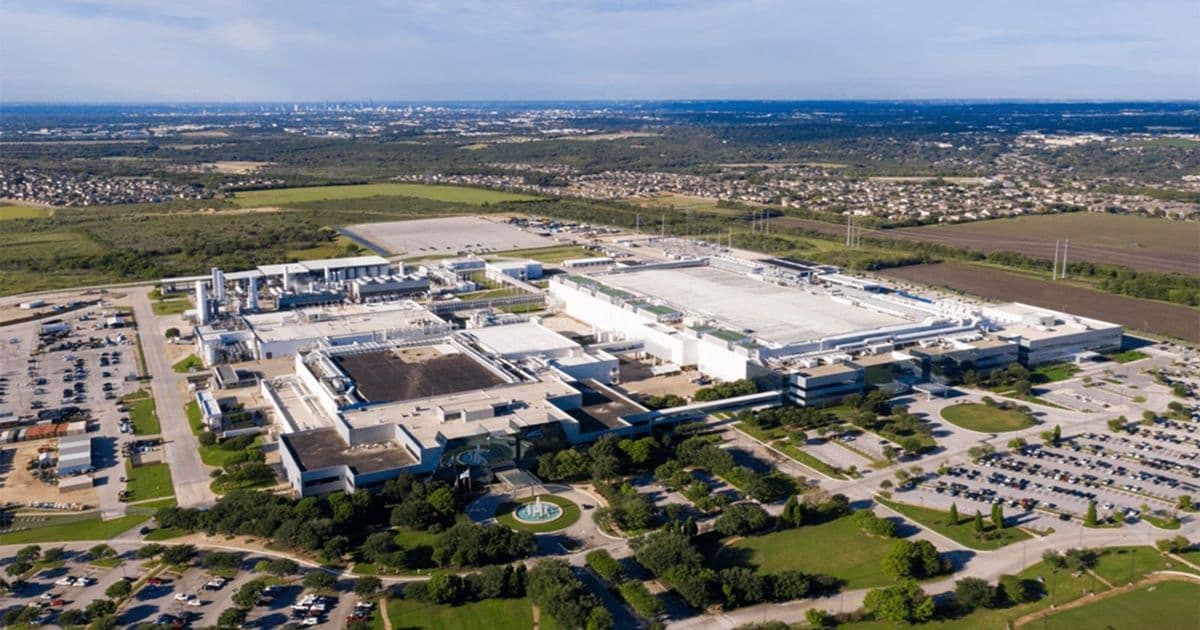
This new facility represents Samsung's most ambitious semiconductor campus to date. Initially announced as a $17 billion project spanning over 5 million square meters (1,235 acres), the investment has since expanded to as much as $44 billion, including two advanced semiconductor fab modules, an advanced packaging facility, and an R&D center. For context, this site is larger than Samsung's domestic South Korea-based campuses near Pyeongtaek and Hwaseong, and dwarfs Intel's Silicon Desert campus near Chandler, Arizona, which covers approximately 700 acres.
(Image credit: Samsung)
The facility's scale is matched by its production ambitions. Samsung is targeting 50,000 wafer starts per month (WSPM) of capacity using the SF2/SF3P process technology at the Taylor fab, according to TrendForce. This capacity significantly exceeds Intel's Fab 52, which offers 40,000 WSPM, and surpasses TSMC's typical fab modules that process around 20,000 WSPM each. While it remains unclear whether this 50,000 WSPM figure applies to the first module alone or the entire $44 billion project, the scale positions Samsung's Taylor facility as potentially the company's largest logic production site ever operated.
A critical technological shift at the Taylor fab involves the implementation of EUV pellicles for the first time in Samsung's manufacturing history. Industry sources indicate that Samsung has ordered dedicated EUV pellicle attachment, detachment, and inspection systems worth approximately 25 billion won ($17.5 million) from FST, a Korean equipment supplier. These production-grade systems are designed to integrate pellicles into a high-volume EUV flow and support both conventional metal-silicide (MeSi) EUV pellicles and next-generation carbon nanotube pellicles.
For those unfamiliar with EUV lithography, a pellicle is an ultra-thin protective membrane mounted above a photomask during exposure to prevent particles from landing on the mask surface and printing defects onto the wafer. While pellicles have long been standard in deep ultraviolet lithography, EUV pellicles present unique challenges due to strict requirements for optical transmission, thermal durability, and mechanical stability under EUV radiation.
Samsung's historical reluctance to adopt EUV pellicles stemmed from several factors. Early EUV pellicles transmitted only around 80% to 88% of 13.5-nm light, causing a 12% to 20% loss of photons when ASML EUV sources operated at around 250W. This photon loss would have significantly reduced wafer throughput and increased cost per wafer due to longer exposure times. Additionally, first-generation pellicles suffered from limited lifetime and thermal instability, warping, cracking, or degrading under sustained EUV radiation, which increased downtime and pellicle failure risk.
(Image credit: Samsung)
Instead of using pellicles, Samsung developed a pellicle-free EUV flow based on ultra-clean mask handling, frequent reticle inspection and cleaning, and short mask reuse cycles. This approach preserved throughput and kept defect risk manageable for smaller dies and few EUV layers. However, the trade-off reportedly included inconsistent yields and variability.
Several factors have now made EUV pellicles more viable for Samsung. ASML has delivered significantly more capable Twinscan NXE:3600D and NXE:3800E machines with more powerful light sources and higher throughput. The industry has also introduced metal-silicide and carbon-nanotube pellicles with better transmittance and durability. Most importantly, the increasing complexity of advanced nodes like SF2/SF3P, which use many more EUV layers than earlier designs, has made pellicles compulsory even for Samsung.
Pellicles sharply reduce stochastic mask-borne defects, which become increasingly dominant at the 2nm scale. For large logic dies, such as Tesla's AI5 chip, a single particle on a critical EUV mask layer can destroy an entire chip or even repeat across multiple fields. By shifting the particle plane out of focus, pellicles dramatically lower this risk, improving yields and, more importantly, yield stability—a critical requirement for clients like Tesla.
The Taylor fab's development has been accelerated by Tesla's commitment to use Samsung Foundry's Texas capacity to build AI6 chips through 2033 and AI5 chips before that. This large customer contract has provided the volume certainty needed for Samsung to proceed with equipment installation and risk production.
Ultimately, the implementation of EUV pellicles at the Taylor fab could represent a breakthrough for Samsung Foundry's position in the competitive semiconductor market. Historically, inconsistent wafer-to-wafer and lot-to-lot yields and performance variability have plagued Samsung's EUV-based nodes, preventing their adoption by clients with larger dies. The Taylor facility's combination of unprecedented scale, advanced EUV pellicle implementation, and high-volume production capabilities may finally address these long-standing challenges and enable Samsung to compete more effectively with industry leaders like TSMC and Intel in the advanced node foundry market.
Comments
Please log in or register to join the discussion