
A detailed investigation into why a temperature-compensated crystal oscillator (TCXO) failed in a high-precision oscilloscope, revealing the dangerous interaction between ultrasonic cleaning and wire bonding processes.
When precision matters, even the smallest components can bring down an entire system. That's exactly what happened when a seemingly routine cleaning process led to the failure of a critical timing component in a high-performance oscilloscope.
The Initial Discovery
Back in January, I received a PCIe version of the ThunderScope prototype open hardware oscilloscope. After some setup challenges involving external GPU enclosures and cable routing, I was finally ready to put it through its paces. I connected it to my Siglent SSG5060X-V vector signal generator and fed it a clean 100 MHz sine wave.
Everything looked promising until I fired up the FFT analysis. Instead of seeing a clean peak at 100 MHz, I found the signal hovering around 106 MHz and drifting slightly. To rule out issues with my signal generator, I measured the 10 MHz outputs from my lab's GPS-disciplined oscillator and rubidium standard directly. Both showed readings of 10.665 MHz instead of the expected 10.000000000 MHz.
The oscilloscope's timebase was running approximately 6.6% slow - a massive error for precision measurement equipment.
Tracing the Problem
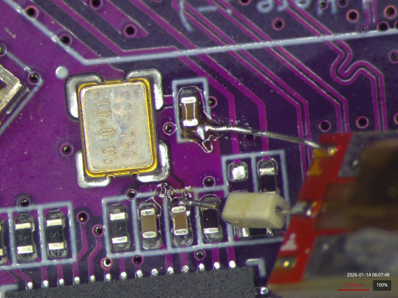
After some debugging, I discovered that the PLL lock bit for the ADC clock generator wasn't engaging. Further investigation revealed that the 10 MHz TCXO (ECS-TXO-3225MV-100) - the primary timebase source - had a flatlined output. The PLL VCO was running wild, with the nominally 1 GHz ADC clock hovering around 938 MHz but unstable.
I reworked the solder joints thinking it might be an assembly defect, but the problem persisted. A replacement TCXO solved the immediate issue, but as someone who can't leave well enough alone, I wanted to understand why the original component failed.
Understanding TCXOs
A TCXO (Temperature Compensated Crystal Oscillator) is designed to maintain frequency stability despite temperature variations. Unlike standard crystal oscillators that drift with temperature changes, a TCXO contains both a quartz crystal and a compensation circuit that actively adjusts the resonant frequency.
The device should contain a quartz resonator, an amplifier circuit, and a temperature compensation circuit - likely integrated into a single IC. When the ThunderScope failed, one of these components or their connections must have broken.
The Cleaning Connection
During discussions with the team, it emerged that the board had been ultrasonically cleaned before being sent to me. This immediately raised red flags. Sonication of MEMS devices and oscillators is notoriously risky because the ultrasonic energy can cause floating structures to resonate at the applied frequency and potentially break.
I advised against ultrasonic cleaning for future units, regardless of whether it turned out to be the root cause. The analysis got delayed for a couple of months due to work commitments, but when I finally examined the failed TCXO, I found something unexpected.
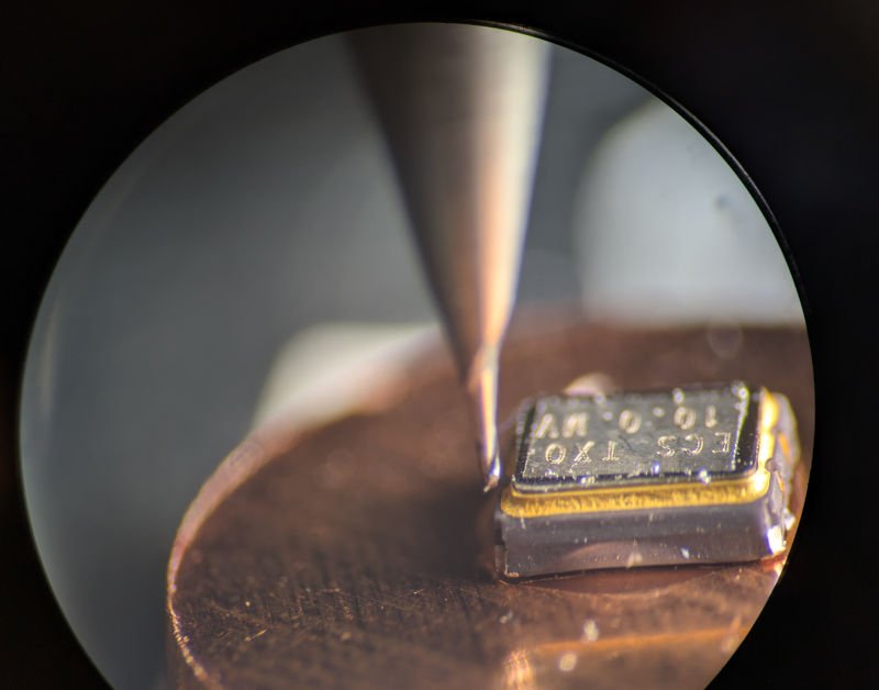
Opening the Package
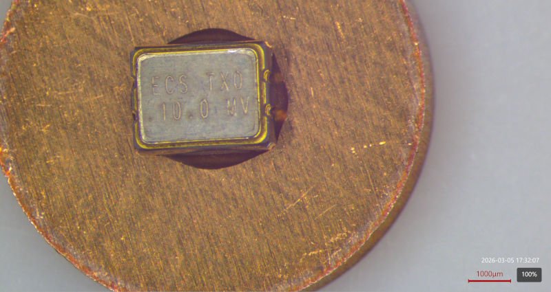
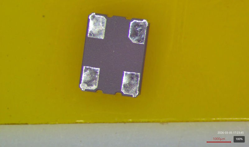
The TCXO is housed in a 3.2 x 2.5 mm hermetically sealed ceramic package with a metal lid. Following MIL-STD-1580D guidelines, I carefully machined through most of the lid, then used a scalpel to make the final cut and peel it back like opening a tin can.
Inside, I found a two-level structure. The quartz crystal was a rectangular sheet with gold electrodes on both sides, attached to gold contacts on the ceramic package with what appeared to be silver-filled epoxy. One edge of the crystal hung over a small rib in the package - possibly an end stop to prevent breakage if dropped.
I spent considerable time inspecting the crystal surface and electrical connections under 20x magnification, looking for fractures, chips, or damage. To my surprise, I found nothing. This was puzzling because I had expected the failure mode of a sonicated quartz oscillator to be "shake the resonator to pieces or rip it off the mount."
Electrical Testing
Before removing the crystal (which would be an irreversible step), I wanted to test its electrical characteristics. Without proper fine-pitch probes, I improvised a setup using SMA cables, pin header adapters, and PCBite probes connected to a VNA.
The measurement setup was far from ideal - insertion loss was around -10 dB due to reflections - but it was sufficient for checking resonance. After some probing, I found what looked like a textbook quartz crystal resonant curve, but centered at 20 MHz instead of 10 MHz.
This suggested there was a divide-by-two circuit in the driver, possibly to improve the duty cycle to a more perfect 50%. More importantly, it indicated that neither the crystal itself nor the electrical connections between it and the package were the source of failure.
Removing the Crystal
I was concerned that the crystal might be rigidly attached and could shatter during removal, but the silver-filled adhesive proved surprisingly soft and broke easily with a scalpel blade. The crystal came out without visible damage under low magnification.
With the crystal removed, I could examine the controller die and its connections more closely.
Controller Die Analysis
The package had three internal levels. The controller die (containing the oscillator driver, temperature compensation, and output divide-by-two) sat in the lowest cavity, attached with a dark adhesive rather than the usual silver-filled epoxy - likely because the package wasn't electrically conductive.
The second level provided electrical contacts connected to the controller via gold ball bonds. The controller die had three bond pads on each side, but the package layout only matched four on one side and two on the other. This mismatch meant one bond wire had to cross over the controller die to reach the far side of the package.
Based on the floorplan, the four corner pins connected to package pins while the two center pins connected to the quartz crystal. All package pins showed reasonable resistance to ground (a few hundred kΩ leakage) when the microscope light was off. Interestingly, there was a strong photoelectric effect - some pins showed negative resistance when the LED ring light shone on the controller die.
This suggested the bond wires to the package pins were likely intact. By elimination, the bonds to the quartz crystal became the primary suspects.
High-Magnification Inspection
I examined the controller die more closely, measuring approximately 645 x 930 μm including scribe lines. The device was made by Asahi Kasei Microsystems, as indicated by the "AKM" logo.
The pinout (counterclockwise from southwest corner) was: output enable, ground, crystal 1, output driver, Vdd, crystal 2. The outer seal ring being output enable was unusual - it's typically ground in most devices I've examined.
The die used a planarized process with three aluminum metal layers. Minimum feature sizes were around 660 nm for metal 1 and 940 nm for metal 3, suggesting a technology node around 250 nm.
While I'm not an expert in analog VLSI layout, I could identify some structures like large capacitors and polysilicon resistors. The layout showed standard cell rows about 9.9 μm tall.
The Critical Finding
The final suspect was the bond wires. It had to be one of the two bonds from the crystal to the controller, since the crystal itself was functioning and the connections to package pins appeared intact.
Under the stereo microscope at a shallow angle, I could see that one of the long bond wires crossing over the controller die was visibly floating above its pad. The wire had separated from the package at the crescent bond interface.
Comparing this to a good bond, the failed connection showed a rough textured surface on the gold contact pad, with the gold wire compressed into a crescent shape by the ball-bonding capillary. The failed bond had a deep circular indentation in the pad that went through the gold into the base metal - something I'd never seen before.
Conclusions
The failure was caused by the long bond wire between the controller die and the substrate trace connecting to one side of the quartz crystal separating from the package at the crescent bond interface. Two factors likely contributed:
- Ultrasonic cleaning: The sonication process probably induced mechanical stress that weakened the bond
- Poor process control: The deep indentation in the pad suggested excessive pressure or ultrasonic power during bonding
After completing the analysis, I learned that a second ThunderScope had failed in exactly the same way after ultrasonic cleaning during rework. While I don't have that failed part to examine, the pattern is strong evidence that sonication was a contributing factor.
This case illustrates how seemingly routine processes like cleaning can interact with manufacturing tolerances in unexpected ways. What might be a marginal but acceptable bond under normal conditions can become a failure point when subjected to additional stress.
For precision equipment manufacturers, this serves as a reminder that component-level cleaning processes need careful consideration, especially for devices with delicate wire bonds and mechanical structures. Sometimes the most sophisticated analysis reveals that the simplest explanation - combined with a bit of bad luck in manufacturing tolerances - is the correct one.
Comments
Please log in or register to join the discussion