
A practical clock-generation pattern from ZipCPU shows why high-speed peripheral interfaces often fail less from headline bandwidth limits than from clocking details, CDC risk, and verification gaps.
ZipCPU is not pitching a funded startup launch here. No funding amount, investor list, or commercial round was disclosed. The traction signal is technical rather than financial: this is a reusable engineering pattern drawn from CPU, DMA, memory-controller, SDIO/eMMC, NAND flash, HyperRAM, and SPI controller work across FPGA and ASIC environments.
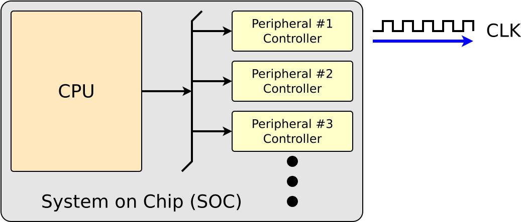
The problem is specific, but common in serious hardware design. Many external peripherals need a clock generated by the master device. That sounds simple until the interface must pause, restart quickly, switch speeds during protocol bring-up, support SDR and DDR timing, avoid clock glitches, and sometimes output a device clock faster than the internal system clock.
A first-pass design often treats the generated device clock as a real internal clock. A counter divides the source clock, a bit of logic gates activity, and user logic runs on posedge dev_clk or even negedge dev_clk. That approach can appear clean in simulation, but it creates an avoidable second clock domain. In FPGA work, the generated clock may not land cleanly on the clock network. In ASIC work, it can still be a maintenance and portability problem, especially if the same IP is expected to run on FPGA prototypes or be sold into FPGA-based systems.
ZipCPU’s article argues for a different model: keep all user logic in the original source clock domain, generate the outgoing device clock as data, and serialize it at the I/O boundary using an ODDR or OSERDES-style output block. The device clock becomes a logic pattern, not a clock that triggers internal state.
That distinction matters because high-speed peripheral protocols are full of awkward timing requirements. SDIO and eMMC may start around 400 kHz, then shift to 25 MHz, 50 MHz, 100 MHz, or 200 MHz depending on the card, PCB, and controller. NAND flash may require a slow initialization phase before a faster operating mode. SPI and Quad SPI controllers may need to pause the clock around chip-select transitions. DDR-style interfaces often need clock transitions centered in the data-valid window, which means a 90-degree phase offset rather than a simple divided clock.

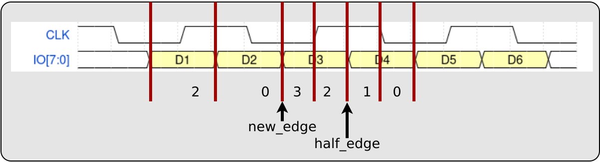
The core technique is to represent the outgoing clock as a wide word. Instead of emitting one clock bit per source-clock cycle, the generator creates a multi-bit pattern such as 0011 or 0110. A normal SDR-aligned clock can use 0011. A DDR clock with a 90-degree offset can use 0110, placing the clock transition in the middle of the data window.

For faster outputs, the same idea scales. With an 8:1 serializer, the design can produce patterns such as 00110011 for a non-offset clock or 01100110 for an offset DDR clock. That allows a 100 MHz source clock to drive a 200 MHz device clock at the pins, while the controller logic itself remains synchronous to the original 100 MHz clock.
The article’s more useful insight is not just the wide clock pattern. It is the companion signaling. The generator emits a new_edge signal when a new device-clock cycle begins and a half_edge signal when the second half of that cycle begins. User logic responds to those strobes while still running on src_clk. In SDR mode, data changes on new_edge. In DDR mode, data can also change on half_edge. This gives the data path timing information without forcing the data path into a generated clock domain.
That model also makes pausing cleaner. If an SD card is streaming blocks into a controller and the system cannot drain buffers quickly enough, the outgoing clock can stop without inventing a new internal timing regime. The clock pattern can be zeroed or held through the pipeline, and the edge strobes stop with it. When the interface is ready again, the clock generator can restart from a controlled phase.
The market positioning here is niche but meaningful. This is the kind of infrastructure that separates hobby-grade peripheral controllers from IP that can survive protocol bring-up, FPGA timing closure, ASIC portability, and formal verification. Companies building storage controllers, embedded SoCs, FPGA-based accelerators, and mixed ASIC/FPGA validation flows all run into this class of problem. The business opportunity is not a flashy consumer-facing layer. It sits in reusable controller IP and verification-heavy hardware design services.
ZipCPU’s skeptical point is that the obvious solution is often the risky one. Dividing a clock with a counter and using the result as a new clock can work in narrow cases, but it invites clock-domain crossings, unexpected skew, hard-to-model clock gating behavior, and awkward DDR handling. A generated clock that looks fine in a pre-synthesis simulation may behave differently once it touches real FPGA clock routing or I/O structures.
The proposed generator handles speed changes by only applying new frequency and phase settings at controlled cycle boundaries. That prevents short pulses and avoids malformed transitions when switching between slow initialization clocks and faster operating clocks. Feedback outputs report the active speed and phase, which is useful for software drivers that need to know when a requested clock change has actually taken effect.
Verification is a large part of the design’s credibility. The article starts with a simple simulation testbench that runs through clock settings from low frequencies up to 200 MHz and checks offset modes. But ZipCPU is candid that waveform inspection is not enough. A non-self-checking testbench can show pretty traces while missing corner cases.
The stronger story is formal verification. The clock generator is paired with an interface property set that describes what downstream transmitter logic may assume: legal wide-clock values, valid combinations of new_edge and half_edge, reset behavior, pending half-cycle rules, and constraints for serializer and ODDR configurations. The generator proof asserts those properties. A transmitter proof can then assume them. That separation reduces the risk of two pieces of logic validating each other through circular assumptions.
There are trade-offs. Supporting multiple hardware output modes, such as 8:1 SERDES, 2:1 ODDR, or neither, increases the number of proof and simulation configurations. High-speed special cases complicate the clock generator. The pattern also depends on the availability and timing behavior of the I/O serialization blocks. Still, the payoff is substantial: one source-clock domain for the controller, controlled output timing at the pad, gated clocks without internal gated-clock logic, and cleaner reasoning about DDR phase alignment.
For teams building FPGA or ASIC peripheral controllers, the lesson is practical. Treat the external clock as an output waveform, not as an internal clocking authority. Keep state transitions under the main system clock. Send timing intent through enables and edge strobes. Push serialization and clock shaping to the I/O boundary, where the hardware is designed to handle it.
The full technical write-up is available from ZipCPU, and the diagrams referenced in the article include the basic SoC peripheral clock relationship, returned-clock interfaces, SDR versus DDR timing, and wide-clock generation patterns. The broader ZipCPU project and related open hardware material can be found through the ZipCPU site and its public code presence on GitHub.
Comments
Please log in or register to join the discussion