
A detailed exploration of a low‑cost, baseband direct‑digital‑synthesis (DDS) signal generator built around a Raspberry Pi Pico, covering architecture, analog front‑end design, PCB fabrication, software, performance measurements, and lessons learned.
Building a Baby DDS Signal Generator: From Concept to Working Instrument
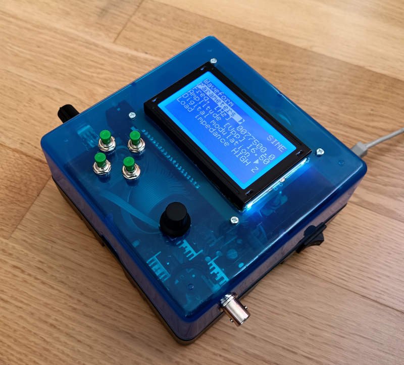
In any modest electronics bench the three pillars are power, scope and signal source. After acquiring a reliable supply and a decent oscilloscope, I set out to create the third – a versatile, precise, and inexpensive base‑band signal generator built around a direct‑digital‑synthesis (DDS) architecture. The result is a self‑contained instrument capable of producing sine, square, triangle and saw‑tooth waveforms from 0.1 Hz up to 1 MHz, with amplitude ranging from 10 mVpp to 20 Vpp (unloaded) and a 50 Ω output stage that can deliver up to 10 Vpp into a matched load.
Core Argument
The central thesis of this project is that a fully functional DDS generator does not require a dedicated DDS IC such as the AD9850. By leveraging a general‑purpose microcontroller (the RP2040 on a Raspberry Pi Pico), an 8‑bit parallel DAC0800, and a modest analog front‑end, one can achieve fine frequency resolution (0.1 Hz steps), amplitude control (10 mV steps), and advanced features like asymmetrical waveforms, AM/ASK modulation, and UART remote control – all for a component cost well below $30.
Key Architectural Blocks
| Block | Main Component | Function |
|---|---|---|
| Digital core | RP2040 (Pico) | Generates the phase accumulator, builds a 1024‑sample wavetable, drives the DAC bus at 8 MHz on core 1, handles UI and UART on core 0 |
| DAC | DAC0800 (8‑bit current‑output) | Converts the digital sample to an analog current; the multiplying architecture permits external amplitude modulation |
| Attenuator | DG408 analog switch + R‑2R ladder | Provides 6 dB steps (0 – ‑42 dB) and fine‑grained level control via a PWM‑derived reference voltage |
| Power amp | Sziklai‑pair push‑pull (Q7/Q8) | Drives the 50 Ω load with low output impedance (≈49 Ω) and up to 24 dBm power |
| User interface | 128×64 monochrome LCD (driven by two 74HC595 shift registers) + rotary encoder + four push‑buttons | Presents menus, frequency, amplitude, waveform, duty‑cycle and limit settings |
| Modulation input | 3.5 mm jack (1 MΩ) + level pot | Accepts external AM signal or digital ASK for DCF77 time‑code transmission |
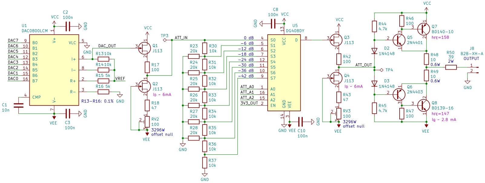
The overall signal path is illustrated in the schematic excerpt below. The first image shows the DAC, attenuator and power‑amp stages as a single block.
Analog Path Details
From DAC to Output
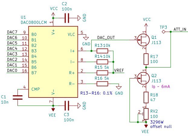
The DAC0800 receives eight data bits from the Pico and produces a current proportional to the digital code. Resistors R13‑R16 set the reference current based on a VREF voltage that is itself derived from a PWM‑filtered output of the Pico. The resulting current is converted to a bipolar voltage at the DAC_OUT node. Because DAC_OUT is high‑impedance, a JFET source‑follower buffers the signal before it reaches the attenuator. The JFET choice (rather than an op‑amp) stems from the need for very high input impedance and a slew‑rate capability that comfortably exceeds the 63 V/µs required for a 20 Vpp, 1 MHz square wave.
Attenuator Ladder
A classic R‑2R ladder, built with 0.1 % resistors, feeds three taps into the DG408 analog switch. The three‑bit selector ATT_A[2:0] chooses a tap, each halving the voltage (‑6 dB). Because the selected tap presents a high impedance, a second JFET follower buffers the attenuated voltage (ATT_OUT) before the power‑amp stage. This arrangement allows the DAC to operate at a comfortable reference current while still providing a dynamic range of over 70 dB after the combined coarse (switch) and fine (PWM) level controls.
Power Amplifier
The final stage is a push‑pull emitter‑follower built from a Sziklai pair. This configuration yields a low output impedance close to the target 50 Ω, while keeping the quiescent dissipation modest. The emitter resistors R48/R49 and R50 set the nominal load impedance to 49 Ω; the transistor collector resistance adds only a fraction of an ohm.
Level Control & Modulation Circuit
Amplitude is set by a 12‑bit PWM output filtered to a DC level (0‑3.3 V). An op‑amp (U2A) amplifies this to 0‑VCC, while a second op‑amp (U2B) buffers the optional external analog input from the 3.5 mm jack. Both signals are summed in U3 to form VREF, the reference voltage for the DAC0800. The TL072, despite its vintage pedigree, offers sufficient bandwidth for the low‑frequency domain and introduces negligible distortion.
PCB Design and Manufacturing
The schematic was first prototyped on a breadboard; once functional, the layout was transferred to KiCAD 9. The board measures 127 × 72 mm to fit inside a translucent blue enclosure that also houses a small mains transformer (re‑purposed from a VCR). Key layout strategies included:
- 8 mil traces for signal lines, widened to 15 mil for power and 40 mil for the 50 Ω output stage.
- Series termination (140 Ω) at the Pico’s DAC and attenuator pins to suppress reflections on the 8‑mil traces.
- “Poor‑man’s dual JFET” – two TO‑92 JFETs shrink‑tubed together to provide thermal coupling and a compact footprint.
The boards were fabricated by PCBWay with a 48‑hour turnaround; the final product arrived in vacuum‑sealed bags with desiccant, and the silkscreen even included a custom “WayWayWay” identifier.
Software Architecture
The firmware resides on the RP2040 and is split across its two cores:
- Core 1 runs a tight loop feeding the DAC FIFO via a PIO state machine at a constant 8 Msps.
- Core 0 handles UI events, UART parsing, menu navigation, and recomputes the wavetable whenever waveform parameters change.
The menu system is data‑driven, making it trivial to add new options. All source code is released under a BSD licence and lives in the project’s GitHub repository (see the src folder for the Pico subdirectory).
Performance Evaluation
Frequency and Amplitude Accuracy
The DDS clock is a crystal‑controlled 8 MHz source, giving a theoretical frequency resolution of 0.1 Hz across the 0.1 Hz‑1 MHz range. Calibration data stored in EEPROM corrects for the slight frequency‑dependent gain error introduced by the attenuator ladder.
Bandwidth and Rise‑Time
Square‑wave edge measurements yielded rise times ranging from 0.33 µs (no attenuation) to 1.0 µs (mid‑range attenuation). Using the rule‑of‑thumb BW ≈ 1/(3·tr) this corresponds to an analog bandwidth of roughly 0.3‑1 MHz. The limitation is not the output stage but the DAC0800 itself; its settling time (≈100 ns) and the parasitic capacitance of the DG408 switch dominate the high‑frequency response.
Spectral Purity
A 4 Vpp sine wave swept in 50 kHz steps showed spurious components around –40 dBc, with most lying below –60 dBc. This matches the expected dynamic range of an 8‑bit DAC (≈48 dB). Total harmonic distortion (THD) stayed in the low single‑percent range, acceptable for most sub‑MHz laboratory work.
Coherent Sampling Effects
Frequencies that are integer multiples of the DAC clock division (e.g., 400 kHz, 500 kHz, 800 kHz, 1 MHz) exhibited markedly cleaner spectra because each output period samples the same phase points – a classic coherent‑sampling phenomenon. Non‑integer relationships produced the usual spectral leakage.
Modulation Capabilities
- AM – By feeding an audio‑range signal into the 3.5 mm jack, the carrier amplitude follows the modulation envelope, as demonstrated with a 1 MHz carrier and a 1‑20 kHz audio tone.
- ASK (DCF77) – The firmware can generate the 77.5 kHz carrier and toggle its amplitude according to the DCF77 time‑code protocol, useful for synchronising radio‑controlled clocks.
Lessons Learned and Future Directions
- DAC choice matters – The DAC0800’s limited bandwidth caps the usable frequency range. Upgrading to a higher‑speed, higher‑resolution DDS chip (e.g., AD9959) would push the usable bandwidth well into the tens of megahertz.
- Attenuator capacitance – The R‑2R ladder combined with the DG408’s switch capacitance introduces a low‑pass effect that reduces bandwidth at intermediate attenuation steps. A resistor‑only step‑attenuator or a digital potentiometer could alleviate this.
- Thermal coupling of JFETs – The shrink‑tube method worked well, but an SMD dual‑JFET would provide tighter matching and smaller board real‑estate.
- Software flexibility – The data‑driven menu makes adding features (e.g., arbitrary waveform upload via UART) straightforward; this is a natural next step.
The project demonstrates that a modest parts list, a bit of PCB craftsmanship, and a microcontroller can produce a capable laboratory instrument. For anyone looking to build a similar generator, the full KiCAD files, Gerbers, BOM, and source code are available in the public repository.
References & Resources
- Full schematic and PCB layout – downloadable PDF (link in repository).
- Raspberry Pi Pico documentation – https://www.raspberrypi.com/documentation/microcontrollers/
- DAC0800 datasheet – https://www.ti.com/lit/ds/symlink/dac0800.pdf
- DG408 analog switch – https://www.ti.com/lit/ds/symlink/dg408.pdf
- TL072 op‑amp – https://www.ti.com/lit/ds/symlink/tl072.pdf
The instrument pictured below is the assembled board inside its blue housing.
End of article.
Comments
Please log in or register to join the discussion