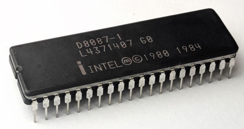
A deep look at the 14‑step microcode sequence that swaps the top‑of‑stack register with any other stack entry in Intel’s original floating‑point co‑processor, including the role of temporary registers, tag bits, and exception handling.
Inside the Intel 8087: How the FXCH Instruction Is Implemented in Microcode
The Intel 8087, introduced in 1980, was the first widely used floating‑point co‑processor. It accelerated arithmetic by up to a hundred times and defined the 80‑bit floating‑point format that still underpins modern CPUs. While most of its instruction set is straightforward, the FXCH (floating‑point exchange) instruction hides a surprisingly rich microcode implementation. The Opcode Collective has reverse‑engineered the 8087’s microcode ROM and uncovered a 14‑step routine that performs the exchange, handles empty registers, and integrates with the chip’s exception system.
The problem FXCH solves
The 8087 stores eight registers in a stack‑like arrangement. Most operations work on the top of the stack (ST(0)). To operate on a value deeper in the stack, programmers use FXCH to swap ST(0) with ST(i). On the surface this looks like a simple register move, but the chip must also preserve tag bits, detect empty registers, and raise the correct exception when needed.
Register layout and tag bits
Each of the eight stack registers holds an 80‑bit floating‑point value: 64‑bit significand, 15‑bit exponent, and a sign bit. Two tag bits accompany every register and indicate whether the entry is valid, special (NaN, infinity, denormal), zero, or empty. The tags are used by the hardware to avoid illegal accesses and to decide how to mask or propagate exceptions.
In addition to the stack, the 8087 has two internal temporary registers, tmpA and tmpB, each with its own tag bits. FXCH uses these temporaries as staging areas.
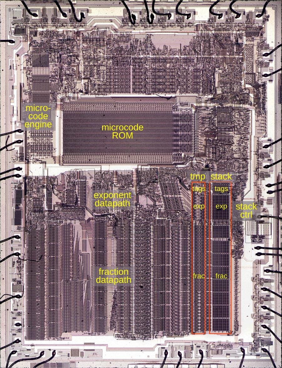 Die of the Intel 8087 with the main functional blocks labeled.
Microcode basics
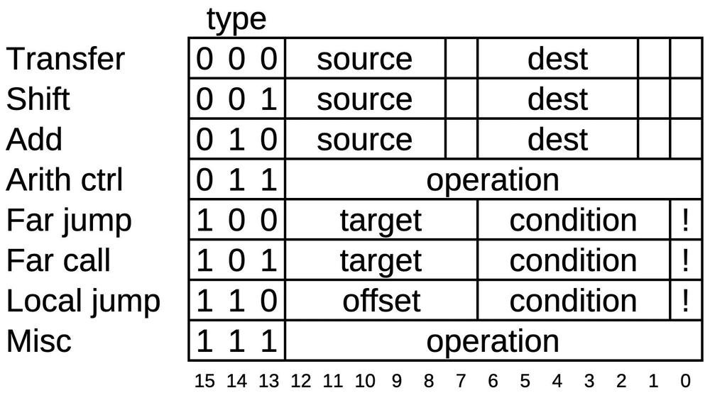
The 8087’s microcode ROM contains 1 648 entries, each 16 bits wide. The first three bits select the instruction class (transfer, shift, arithmetic, control, etc.). The remaining bits encode source and destination fields, condition codes, or jump offsets. A typical transfer micro‑instruction moves data between internal buses and registers.
The 14‑step FXCH routine
Below is the micro‑address sequence (hex) together with a brief description of each step. The notation ST(0) -> tmpA means “read the top‑of‑stack value and store it in temporary A”.
| Addr | Micro‑instruction | Meaning |
|---|---|---|
| 0200 | ST(0) -> tmpA |
Capture the top value and its tag bits. |
| 0201 | nop |
One‑cycle wait for bus stability. |
| 0202 | ST(i) -> tmpB |
Read the selected stack entry (i comes from the FXCH opcode). |
| 0203 | if !(tmpA.empty or tmpB.empty) jmp 0210 |
Conditional jump to the fast path when both registers contain data. |
| 0204 | set invalid exception |
Raise an invalid operation if either register is empty. |
| 0205 | if (unmasked) jmp 0213 |
If the exception is not masked, abort the routine and let the 8086 handle the interrupt. |
| 0206 | if !tmpA.empty jmp 0208 |
Test tmpA; if it is not empty, skip the NaN substitution. |
| 0207 | NaN -> tmpA |
Replace an empty tmpA with the special NaN pattern. |
| 0208 | if !tmpB.empty jmp 0210 |
Same test for tmpB. |
| 0209 | NaN -> tmpB |
Substitute NaN for an empty tmpB. |
| 0210 | tmpB -> ST(0) |
Write the (possibly substituted) value back to the top of the stack. |
| 0211 | nop |
Cycle‑level timing buffer. |
| 0212 | tmpA -> ST(i) |
Store the original top‑of‑stack value into the target position. |
| 0213 | RNI |
End of micro‑routine; return control to the 8086. |
| 0214‑0216 | nop |
Unused slots, likely left over from an earlier, longer implementation. |
The routine can be split into three logical paths:
- Happy path – both registers are present, the routine jumps directly from 0203 to 0210.
- Exception path – an empty register triggers the invalid operation exception at 0204. If the exception is masked, the microcode substitutes NaN (steps 0206‑0209) before proceeding.
- Interrupt path – if the exception is unmasked, the microcode exits at 0213, letting the 8086 service the interrupt.
Why the nop instructions?
The 8087’s datapaths for exponent/sign and significand run on separate buses. After a read or write, the bus must settle before the next operation. The nop micro‑instructions provide the required one‑cycle delay. The three trailing nops (0214‑0216) appear to be unused space; they may be remnants of a longer version of the routine that was trimmed during tape‑out.
Exception handling in detail
When an empty register is detected, the microcode sets the invalid operation flip‑flop. The control register contains a mask bit for each of the six exception classes (invalid, denorm, zero‑divide, overflow, underflow, precision). If the mask for invalid is clear, the flip‑flop propagates to the status register and an interrupt line is asserted to the 8086. If the mask is set, the microcode continues and replaces the missing value with a predefined NaN pattern (exponent all 1’s, fraction bits zero except for the top two bits). This behavior matches the Intel documentation for “masked” exceptions.
Extracting the microcode
The 8087’s ROM stores two bits per transistor, using four voltage levels. After stripping the metal layers, the Opcode Collective photographed the array, then applied a neural‑network classifier to label each transistor size. Mapping the transistor grid to logical bits required untangling row/column shuffles introduced for layout density. The final bit‑stream was decoded into the 1 648 micro‑instructions shown above.
The full ROM image and the decoded table are available in the public repository:
- 8087 microcode repository on GitHub
- High‑resolution die photos:
What this tells us about the 8087 design
- Microcode density – 14 words for a register exchange may seem excessive, but the routine also embeds exception detection, masking logic, and timing buffers. The designers favoured a uniform microcode engine over hard‑wired shortcuts.
- Tag‑aware data path – By moving the tag bits along with the value, the microcode keeps the stack’s state consistent without extra hardware.
- Flexibility for future extensions – The conditional jumps and spare nop slots suggest the engineers left room for later instruction variants or bug fixes.
Continuing the reverse‑engineering effort
FXCH is only one of many complex instructions. The Opcode Collective is still decoding arithmetic kernels, trigonometric functions, and the floating‑point divide unit. Each new insight refines our understanding of how early micro‑architects balanced silicon limits with functional richness.
Follow the progress on:
- Bluesky: @righto.com
- Mastodon: @[email protected]
- RSS feed linked from the GitHub repo.
This article was written without the use of AI‑generated text.
Comments
Please log in or register to join the discussion