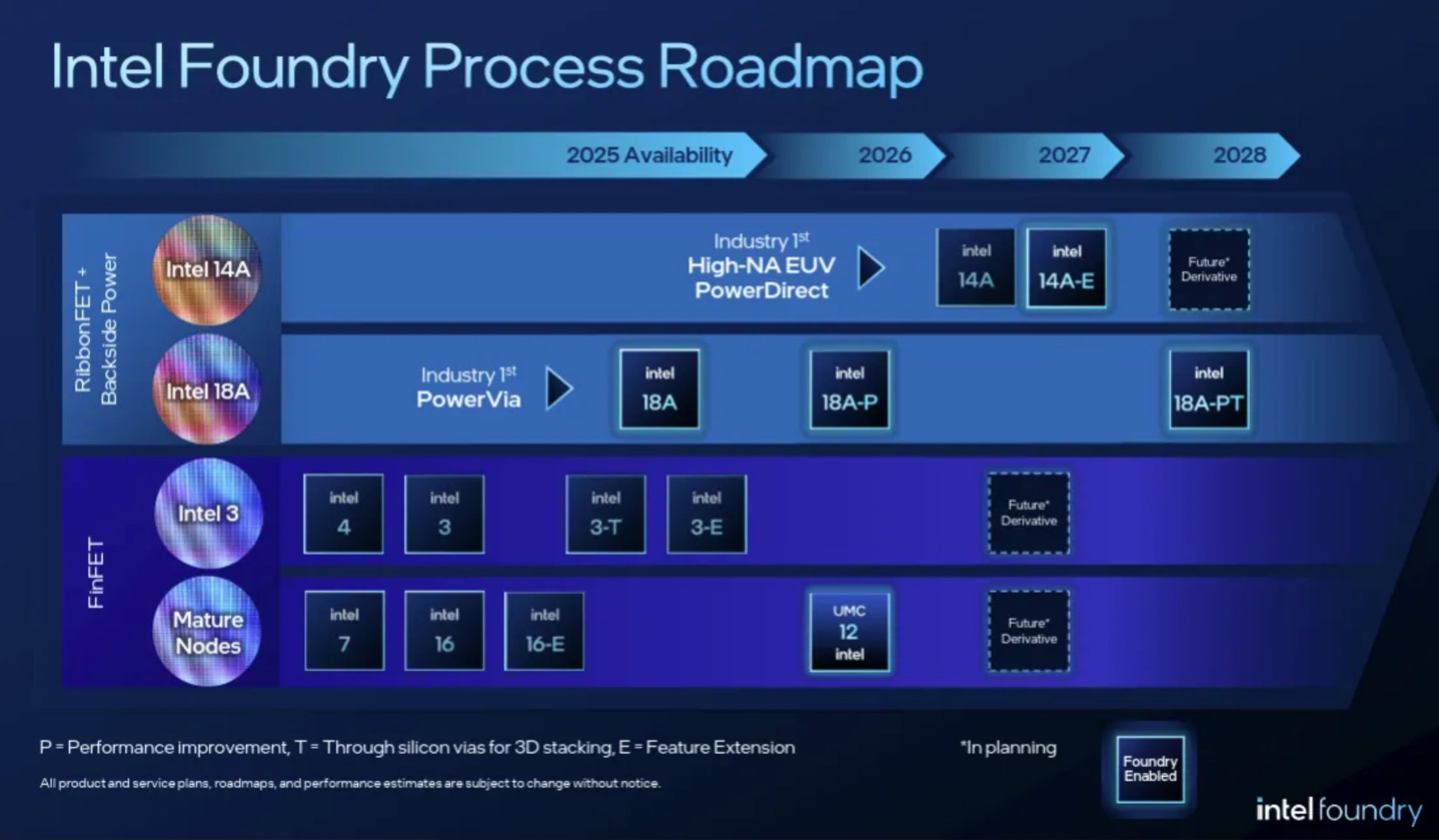
Intel's advanced 14A fabrication process is moving from development to customer engagement, with two external companies currently evaluating test chips. While no formal commitments exist yet, Intel's leadership expects firm supplier decisions to begin in the second half of 2026, setting the stage for production ramp in 2028. The foundry is preparing its PDK 0.5 for release this quarter and developing multiple process variants to address different market segments and cost structures.
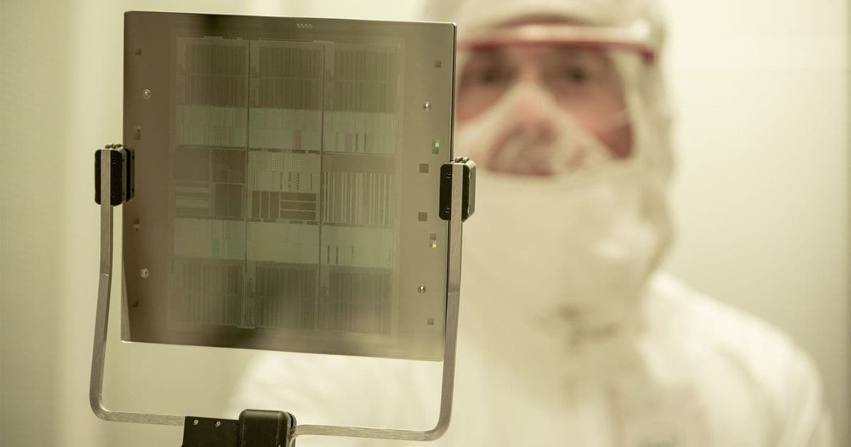
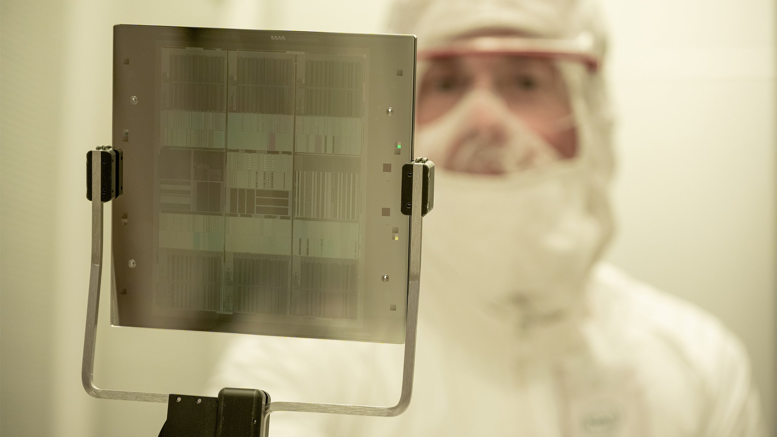
Intel's foundry business has reached a critical milestone in its pursuit of external customers for its next-generation 14A manufacturing process. According to disclosures made during the company's recent earnings call, two prospective customers are currently evaluating test chips fabricated on Intel's 14A process technology. This represents the first tangible evidence of external interest in Intel's most advanced node, though the company remains cautious about projecting immediate commitments.
"A couple of customers we are already engaging about the PDK version 0.5, they are [also] looking at the test chip [and] more importantly, a specific product they are going to run [at] our foundry and that one we are working with them," said Lip-Bu Tan, chief executive of Intel, during the earnings discussion. "Engagements with potential external customers on Intel 14A are active, and we believe customers will begin to make firm supplier decisions starting in the second half of this year, and extending into the first half of 2027."
The current situation reflects the typical foundry customer engagement cycle, where chip designers evaluate process technology through test chips before committing to production capacity. Intel has no external customer commitments for 14A at this time, which aligns with the company's stated policy of keeping capital expenditures minimal until firm demand materializes. This approach contrasts with Intel's historical model as an integrated device manufacturer, where internal product needs drove process development and capacity investment.
The timeline for customer decisions and subsequent production ramps follows industry standards for advanced node adoption. If customers commit to 14A in the second half of 2026, they would be positioned to ramp production of their designs in 2028. This two-year lead time accounts for the complete design cycle, including PDK finalization, IP integration, design validation, and the physical manufacturing ramp.
"We think that in the second half of this year, they are going to indicate to us what kind of capacity, firm commitment, so that we can deploy the capacity, CapEx, to really build that [capacity they need]," Tan explained. "I think it is a service business. We already give the trust and the consistency we are able to deliver."
PDK Development and Industry Standardization
A critical component of foundry success is the process design kit (PDK), which provides chip designers with the necessary tools, models, and rules to develop integrated circuits for a specific manufacturing process. Intel revealed that it is on track to release 14A PDK version 0.5 later this quarter, a milestone that typically marks the point where serious chip design work can begin.
"Intel 14A development remains on track and we have taken meaningful steps to simplify our process flow and improve our rate of performance and yield improvement," Tan added. "We are developing a comprehensive IP portfolio on Intel 14A, and we continue to improve our design enablement approach. Importantly, our PDKs are now viewed by customers as industry standard."
The emphasis on PDK standardization is significant. In the foundry industry, customers often design for multiple foundries simultaneously, and a PDK that closely matches industry standards reduces the learning curve and design porting time. Intel's claim that its PDKs are now viewed as industry standard suggests the company has made substantial progress in aligning its design enablement tools with what chip designers expect from TSMC and Samsung Foundry.
Multiple Process Variants for Market Segmentation
Intel's approach to 14A extends beyond a single process variant, indicating the company is developing the technology with diverse customer requirements in mind. When asked about the use of ASML's Twinscan EXE High-NA lithography tools for 14A, Intel's CFO David Zinsner noted, "Of course, there will be different variants of 14A, but High-NA is targeted [for insertion into] 14A [flow]."
This statement opens several possibilities for process segmentation. Different variants could address different market segments with varying requirements for transistor density, power efficiency, and cost:
High-performance variants would likely incorporate ASML's High-NA EUV lithography ($400 million per scanner) to achieve maximum transistor density for leading-edge CPUs, GPUs, and AI accelerators.
Cost-optimized variants for mobile or IoT applications might skip High-NA lithography, using existing EUV tools instead to reduce manufacturing costs while still delivering competitive performance.
Specialized variants could exclude certain features like backside power delivery networks (BPDN) for applications where power delivery requirements are less stringent.
This segmentation strategy mirrors approaches used by leading foundries like TSMC, which offers multiple versions of each process node (N5, N5P, N4, N4P, etc.) tailored to different performance and power targets.
The Competitive Landscape and Intel's Position
Intel's 14A process represents the company's most advanced node in its aggressive roadmap to regain process leadership by 2025. The process is expected to deliver significant improvements in transistor density, performance, and power efficiency compared to Intel's current 18A node, which is scheduled for production in 2025.
For external customers, 14A offers an alternative to TSMC's N2 process (scheduled for 2025) and Samsung's 2nm node. Intel's value proposition includes:
- Geographic diversification: For customers concerned about concentration risk in Taiwan, Intel's U.S. and European fabs provide supply chain resilience.
- Advanced packaging integration: Intel's EMIB and Foveros technologies could offer unique integration capabilities for heterogeneous chip designs.
- Process innovation: Intel's RibbonFET transistor architecture and PowerVia backside power delivery could deliver competitive advantages.
However, Intel faces significant challenges in attracting external customers. TSMC dominates the foundry market with approximately 60% share and has established trust through decades of consistent execution. Samsung Foundry holds approximately 13% share and offers competitive process technologies. Intel must demonstrate not only technical parity but also consistent yield, volume production capability, and customer service excellence.
Financial Implications and Capital Deployment
Intel's cautious approach to capacity investment reflects the capital-intensive nature of semiconductor manufacturing. Building a new fab capable of producing advanced nodes requires billions in investment, with EUV and High-NA tools representing major cost components. By waiting for firm customer commitments before deploying capacity, Intel aims to minimize financial risk while demonstrating fiscal discipline to investors.
This approach contrasts with Intel's historical model as an integrated device manufacturer, where internal product needs (CPUs, chipsets, etc.) drove capacity planning. The transition to a foundry model requires a fundamental shift in how Intel evaluates return on investment, with customer commitments becoming the primary driver for capacity expansion.
Timeline and Next Steps
The next 18 months will be critical for Intel's foundry ambitions:
- Q1 2025: Release of 14A PDK 0.5
- H2 2025: Customer decisions on 14A commitments expected
- 2026: Capacity planning and initial tool installation for committed customers
- 2027: Process qualification and initial production
- 2028: Volume production ramp for external customers
Intel's success in attracting external customers to 14A will serve as a key validation of its foundry strategy and its ability to compete with established players. The company's recent earnings disclosures suggest that while interest exists, the foundry business remains in its early stages, with the next 12-18 months determining whether Intel can translate technical development into commercial success.

For now, the two prospective customers evaluating 14A test chips represent a promising start, but Intel must convert this interest into firm commitments and eventually, revenue-generating production. The semiconductor industry will be watching closely to see if Intel can execute its foundry vision and establish itself as a viable alternative in the advanced manufacturing landscape.
Comments
Please log in or register to join the discussion