AMD's Instinct MI355X AI GPU achieves 2x per-CU throughput with 32 compute units versus 38 in MI300X, while matching Nvidia's GB200 performance in MLPerf benchmarks despite lower complexity and cost.
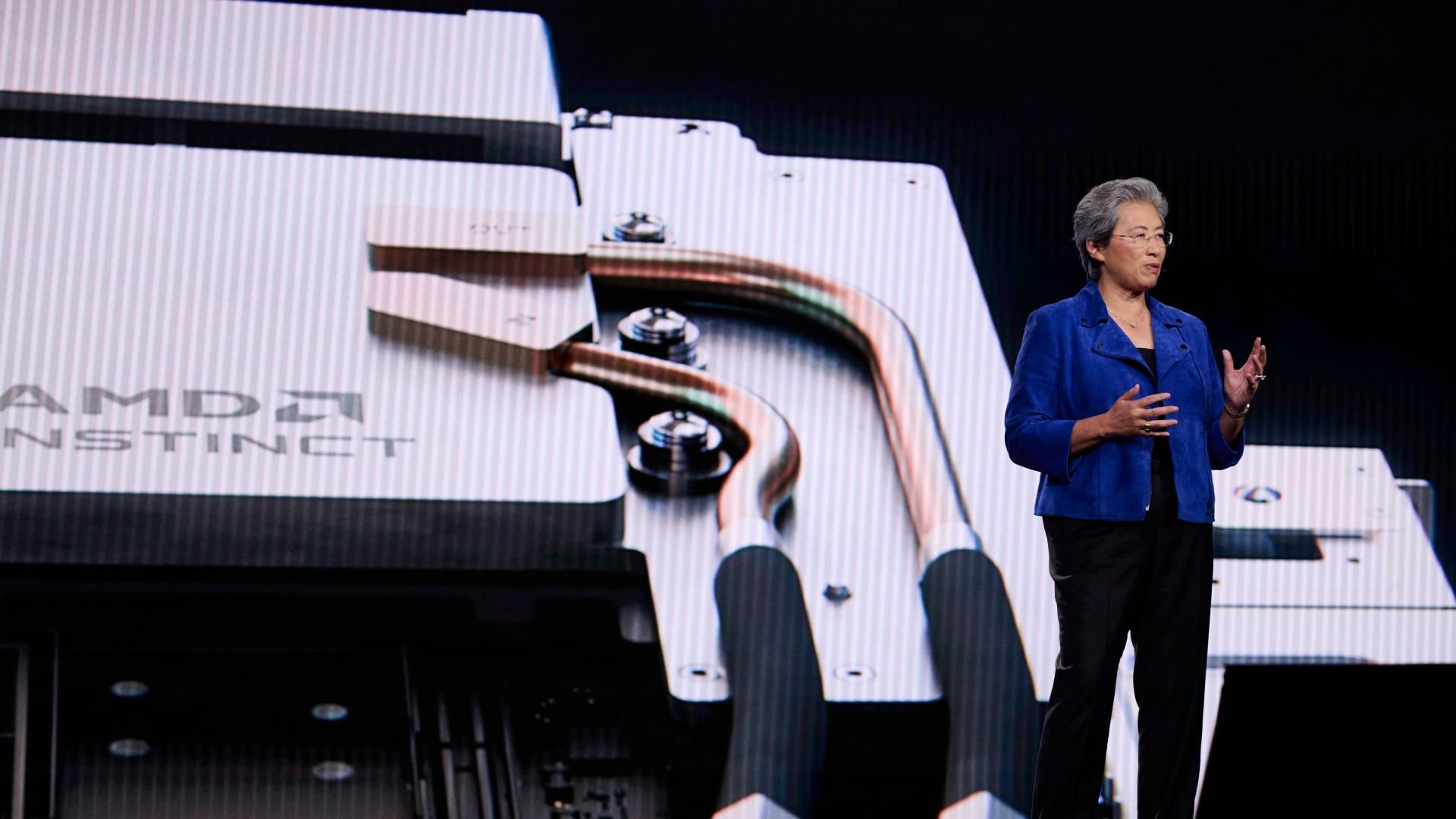
At the IEEE International Solid-State Circuits Conference (ISSCC) 2026, AMD fellow design engineer Ramasamy Adaikkalavan revealed the engineering breakthroughs behind the Instinct MI355X AI GPU that enable it to deliver nearly double the compute throughput while using fewer compute units than its predecessor.
Fewer Compute Units, More Performance
The MI355X represents a counterintuitive approach to AI accelerator design. While the MI300X featured 38 compute units per Accelerator Complex Die (XCD), the MI355X reduces this to 32 active compute units. However, AMD doubled per-CU FP8 throughput from 4,096 FLOPS per clock to 8,192 by redesigning the matrix execution hardware rather than simply adding more units.
This architectural decision stems from AMD's "selective sharing strategy" for numeric format hardware. Instead of building entirely dedicated hardware for each numeric format (which is expensive in die area) or sharing all hardware across every format (cheaper but inefficient), AMD analyzed each arithmetic component individually and shared only where the power penalty was acceptable.
Process Node Advancements and Power Efficiency
The transition from TSMC's N5 to N3P process node brought both opportunities and challenges. While logic density continues to scale linearly, routing density hasn't kept pace, creating a growing back-end-of-line problem. AMD addressed this by adding two additional metal routing layers, increasing the metal stack from 15 to 17 layers.
At 3nm, wiring now accounts for a larger fraction of total switching power than in prior generations. AMD's response included careful floorplan optimization and ML-based placement algorithms to minimize wire length on active signal nets. Combined with custom activity-based clock gating cells that detect and shut off unnecessary clock toggling for repeated zero or one data streams, AMD targeted a greater than 30% reduction in process-neutral switching capacitance per operation compared to the MI300X's XCDs.
I/O Die Redesign and Memory Bandwidth
AMD consolidated the MI355X's I/O dies from four separate dies in the MI300X to two larger dies that are directly connected to each other. This consolidation delivers meaningful efficiency gains beyond simply reducing die count. Fewer die-to-die crossings enabled AMD to remove circuitry previously required to handle domain crossings and protocol translations.
The freed-up area went into widening the Infinity Fabric data pipeline, allowing peak HBM bandwidth to be delivered at lower operating voltages and frequencies. AMD claims 1.3x better HBM read bandwidth per watt compared to the MI300X, with raw bandwidth increasing 1.5x (from 5.3 to 8.0 TB/s). The efficiency gain came from running the fabric at a less power-hungry operating point.
Local Data Share and Memory Architecture
The MI355X features a substantially larger Local Data Share (LDS) compared to the MI300X-series. At 160KB per compute unit versus 64KB, with double the bandwidth, the expanded LDS improves utilization of the newly expanded matrix compute unit through extensive on-chip data reuse. During matrix multiply-accumulate operations, the LDS feeds data directly to the matrix compute units, and the larger LDS reduces how often the GPU must reach out to slower memory tiers to reload operand data.
AMD also added a direct LDS load path from the L1 data cache that eliminates intermediate register usage, further reducing memory latency for these operations.
Performance Benchmarks and MLPerf Results
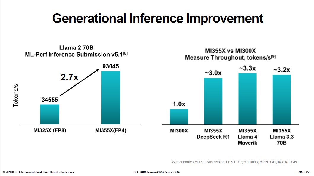
In MLPerf Inference v5.1, the MI355X achieved 93,045 tokens per second on the Llama 2 70B benchmark—a 2.7x improvement over the MI325X. Internal throughput comparisons running FP4 inference against the MI300X's FP8 results showed roughly a threefold improvement in token generation across DeepSeek R1, Llama 4 Maverick, and Llama 3.3 70B.
However, these figures come with important caveats. The FP4 versus FP8 comparison doesn't isolate hardware from software and data format improvements, as the MI300X never supported FP4. Similarly, the training comparison against Nvidia's GB200 shows the MI355X completing a Llama 2 70B LoRA fine-tuning run in 10.18 minutes versus 11.15 minutes for the GB200—about 10% faster. AMD's result came from MLPerf Training v5.1 using FP4, while the Nvidia figure is the GB200's last published FP8 score from MLPerf Training v5.0; Nvidia has not submitted a comparable FP4 training result.
Adaikkalavan was candid about what the parity result reflects: "We are actually matching the performance of the more expensive and complex GB200. It tells you a couple of things. One, we have strong hardware, which we always knew. And second, the open software frameworks have made tremendous progress."
Memory Capacity and Form Factor
AMD's reckoning shows the MI355X carries 288GB of HBM3E against the B200's 192GB, and delivers roughly double the FP64 throughput—2.1x compared to the B200. For general inference workloads, the two accelerators are at rough parity, with the MI355X's larger memory pool providing its most consistent advantage for running large models without distributing them across multiple GPUs.
Both the MI350X (1,000W TBP, 2,200 MHz) and the flagship MI355X (1,400W TBP, 2,400 MHz) maintain the same physical form factor as the MI300X. AMD built this constraint into the project from the start, designing the entire CDNA 4 generation to function as a drop-in infrastructure upgrade for existing MI300-based servers rather than requiring new rack designs or cooling infrastructure.
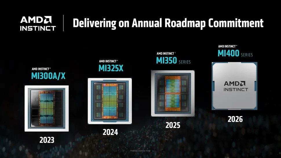
Looking Ahead: The MI400 Series
With the MI400-series waiting in the wings, the MI350 series will soon play second fiddle. The MI400 is built on TSMC's N2 process, with 432GB of HBM4 and roughly double the compute. AMD continues to promise those chips for the second half of this year.
However, in a world where every AI FLOP is potentially valuable, both AMD and its customers will likely continue to optimize performance on the MI350 family for some time to come. The engineering decisions behind the MI355X—particularly the selective sharing strategy and the focus on power efficiency through careful floorplanning and clock gating—demonstrate AMD's maturing approach to AI accelerator design, one that balances raw performance with practical considerations like die area, power consumption, and software ecosystem compatibility.

Comments
Please log in or register to join the discussion