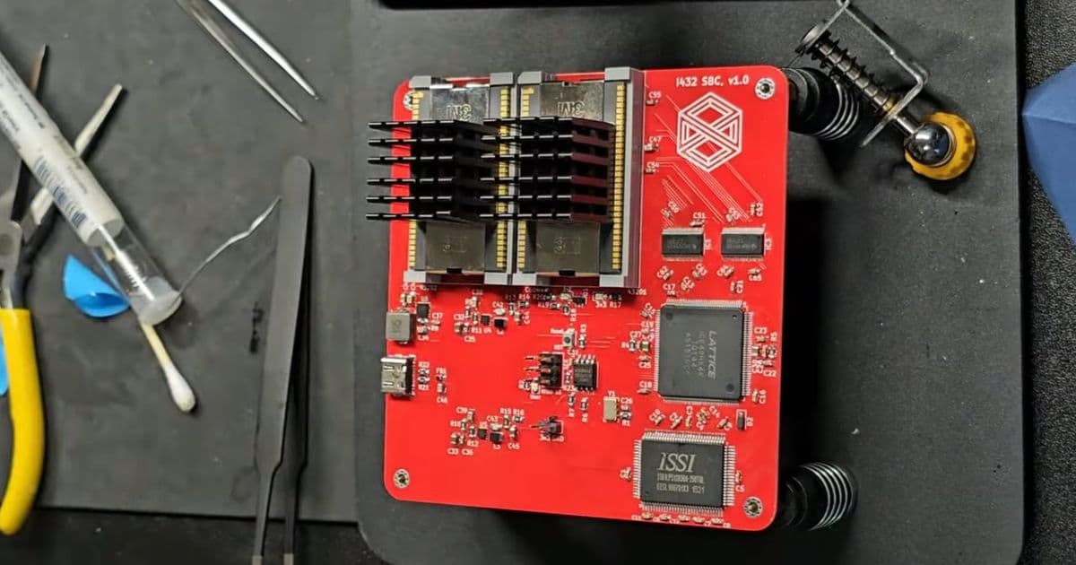
A new single‑board computer built around Intel’s notorious iAPX432 shows that the chip’s poor performance may have stemmed more from compiler and system‑level shortcomings than from its radical architecture, prompting a fresh look at this hyper‑CISC experiment.
Introduction
When the 1980s saw most manufacturers converging on reduced‑instruction‑set designs, Intel took a daring detour with the iAPX432 – a processor that tried to embed high‑level language concepts directly into hardware. The result was a three‑chip system that promised object‑oriented instructions, type safety, and a rich instruction set of more than two hundred operators, yet it quickly earned a reputation for sluggishness and excessive heat dissipation. Recent work by hobbyist engineer Mark The Quasi‑Engineer challenges the prevailing narrative, suggesting that the chip’s failures were not inevitable but rather the product of a weak software stack and sub‑optimal system design.
The Architecture in a Nutshell
The iAPX432 was split into two General Data Processor (GDP) chips and a third chip dedicated to I/O. Unlike conventional CPUs, it lacked any directly addressable general‑purpose registers; instead, all data lived in objects stored in memory, and the processor manipulated these objects through a complex addressing scheme that supported both direct and indirect references. This model was meant to free programmers from manual register allocation and to enforce type safety at the hardware level.
Key characteristics:
- Object‑oriented instruction set – operations such as
CALL_METHODandCREATE_OBJECTwere native. - 200+ opcodes – many performed multi‑step actions that would normally require several instructions on a RISC core.
- No visible registers – the programmer interacted with handles to memory‑resident objects.
- Dual‑GDP design – two parallel pipelines intended to boost throughput for the heavily micro‑coded instruction set.
The ambition was clear: make the machine behave like a high‑level language runtime. In theory, this could reduce the instruction count for complex tasks dramatically.
Building a Modern Testbed
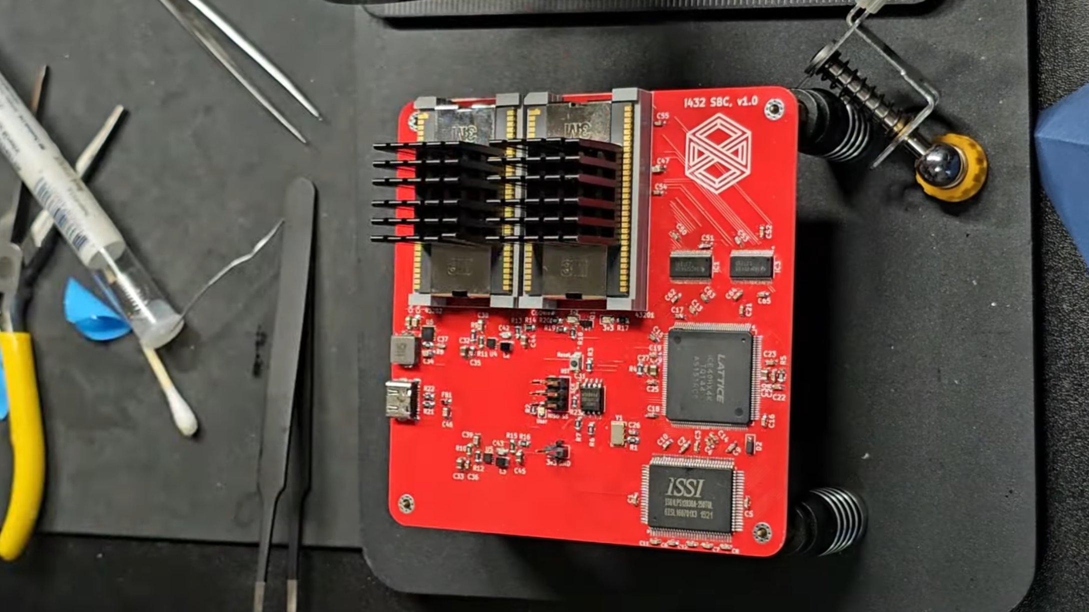
To evaluate the chip today, Mark constructed a single‑board computer (SBC) that houses the two GDP chips and an FPGA that provides modern I/O capabilities. The design files and firmware are available on his GitHub repository. The board also includes a voltage regulator that was redesigned after the original component failed under the chip’s notorious power draw.
The SBC’s architecture mirrors the original system but replaces the antiquated peripheral interfaces with contemporary UART, SPI, and USB‑over‑FPGA bridges, allowing the iAPX432 to communicate with a host PC for program loading and result extraction.
The Benchmark: Spigot Algorithm for Pi
Mark chose the Spigot algorithm – a digit‑by‑digit method for generating π – because it stresses integer arithmetic, memory accesses, and control flow without relying on floating‑point hardware (which the iAPX432 lacks). He hand‑coded the algorithm in the processor’s native assembly, deliberately using direct addressing to avoid the extra cycles incurred by indirect modes.
Results
| Processor | Digits of π | Execution Time |
|---|---|---|
| iAPX432 (hand‑coded) | 2048 | 1.0 × (baseline) |
| Intel 8086 (hand‑coded) | 2048 | 2.5 × (baseline) |
Surprisingly, the iAPX432 outperformed the 8086 by a factor of 2.5, despite the latter’s simpler instruction set and lower clock speed. The result contradicts the long‑standing belief that the 432 was uniformly slower than any contemporary CISC design.
Why the Original Chip Fell Short
Mark’s findings point to two primary culprits behind the historical disappointment:
- Compiler and Toolchain Deficiencies – The original Intel development environment produced code that relied heavily on the processor’s indirect addressing and on the heavyweight object‑creation instructions, inflating cycle counts. Modern hand‑optimised assembly can sidestep these pitfalls, as demonstrated.
- System‑Level Bottlenecks – Early motherboards used rudimentary voltage regulation and limited bus bandwidth, causing the GDP chips to stall frequently. The new SBC’s clean power supply and fast FPGA‑mediated I/O eliminate many of those stalls.
In essence, the iAPX432’s hardware was not intrinsically incapable; rather, the surrounding software ecosystem failed to exploit its unique capabilities.
Implications for Modern Architecture
The iAPX432 story resonates with current trends in domain‑specific architectures (DSAs) and hardware‑accelerated runtimes. Today’s GPUs, TPUs, and even emerging WebAssembly‑centric CPUs embed higher‑level abstractions directly into silicon, hoping to reduce the “semantic gap” between software and hardware. The lesson from the 432 is clear: without a mature compiler stack and well‑engineered system integration, even a theoretically powerful ISA can languish.
Moreover, the experiment underscores the value of hardware‑software co‑design. Modern projects such as RISC‑V extensions for vector processing or custom accelerators for machine learning succeed because the compiler, runtime, and hardware are developed in lockstep, something Intel lacked for the 432.
Counter‑Perspectives
Critics may argue that hand‑optimised assembly is an unfair comparison; after all, most developers never write raw machine code. If the iAPX432 had received a robust optimizing compiler akin to today’s LLVM back‑ends, perhaps its performance would have been competitive on a broader range of workloads. Conversely, the sheer complexity of its instruction set still imposes a higher micro‑code overhead than a lean RISC core, meaning that for compute‑bound tasks without heavy object manipulation, a simpler ISA would likely remain superior.
Conclusion
The renewed interest sparked by Mark’s SBC and benchmark invites a more nuanced view of the Intel iAPX432. While the chip’s architectural ambition was ahead of its time, the surrounding software and hardware ecosystem failed to deliver the promised performance. As the industry revisits the idea of embedding high‑level semantics in silicon, the iAPX432 serves as both a cautionary tale and a source of inspiration: hardware can be powerful, but only when the software that drives it is equally sophisticated.
For a deeper dive into the SBC schematics, see the design notes.
Related reading: The ill‑fated Itanium project, another Intel attempt to leapfrog conventional designs, shares a similar narrative of ambition outpacing ecosystem readiness.
Comments
Please log in or register to join the discussion