
MIT researchers developed a fabrication method that creates matched 'fingerprints' on paired chips, enabling direct mutual authentication without storing cryptographic secrets on vulnerable third-party servers.
Physical unclonable functions (PUFs) leverage microscopic manufacturing variations in CMOS chips to create unique identifiers analogous to human fingerprints. These hardware-based security features offer robust protection against counterfeiting and unauthorized access. However, conventional PUF implementations require storing reference data on external servers—creating security vulnerabilities while adding computational overhead and memory requirements.
MIT engineers have now solved this limitation with a novel fabrication technique that creates mathematically correlated PUFs on paired chips during manufacturing. As lead researcher Eunseok Lee explains: "All the secrets remain safe inside the silicon. We don't need to store any information externally."
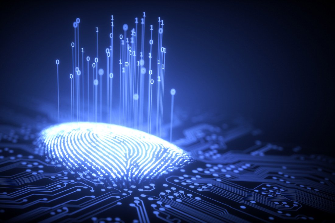
 The unique patterns visible on each chip (shown here as a 'fingerprint') emerge from unavoidable microscopic variations during semiconductor fabrication.
The method exploits gate oxide breakdown—an intentional degradation process—to create shared cryptographic keys. During fabrication:
- Transistor pairing: Two transistor pairs are fabricated along adjacent edges of chips still connected on the silicon wafer
- Controlled breakdown: Low-cost LEDs apply high voltage until one transistor in each pair breaks down
- Shared randomness: Manufacturing variations cause unique breakdown timing, recorded via metal interconnects
- Separation: Chips are diced between transistor pairs, preserving correlated breakdown states
This creates a matched PUF pair where each chip contains complementary cryptographic information. When authenticating, chips directly verify each other using challenge-response protocols based on their shared physical characteristics. No external database stores secret keys—eliminating server-side attack vectors.
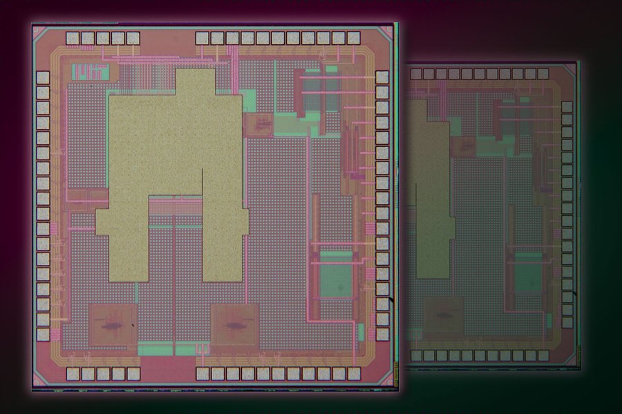 Microscopic view of chip structures showing randomized patterns that form the basis of physical unclonable functions.
Testing demonstrated 98% reliability in key matching between paired chips. The approach maintains compatibility with standard CMOS processes and requires no special materials, keeping costs low. Key advantages include:
- Enhanced security: Secrets never leave silicon substrate
- Energy efficiency: Minimal computation vs traditional PKI
- Scalability: Leverages existing semiconductor workflows
Applications target systems with non-interchangeable hardware pairs:
- Medical sensor pills communicating with wearable monitors
- Industrial IoT controller/sensor pairs
- Secure hardware handshakes in autonomous vehicle components
Current implementations convert analog breakdown patterns into digital keys. Future work aims to preserve the raw analog physical characteristics for stronger security. As co-author Ruonan Han notes: "We're exploring how more complex, analog-based secrecy can be duplicated—and only duplicated once."
The Terahertz Integrated Electronics Group and Energy-Efficient Circuits and Systems Group continue developing this approach with support from Lockheed Martin and academic fellowships. This hardware-rooted security paradigm could fundamentally reshape authentication in resource-constrained edge devices.
Comments
Please log in or register to join the discussion