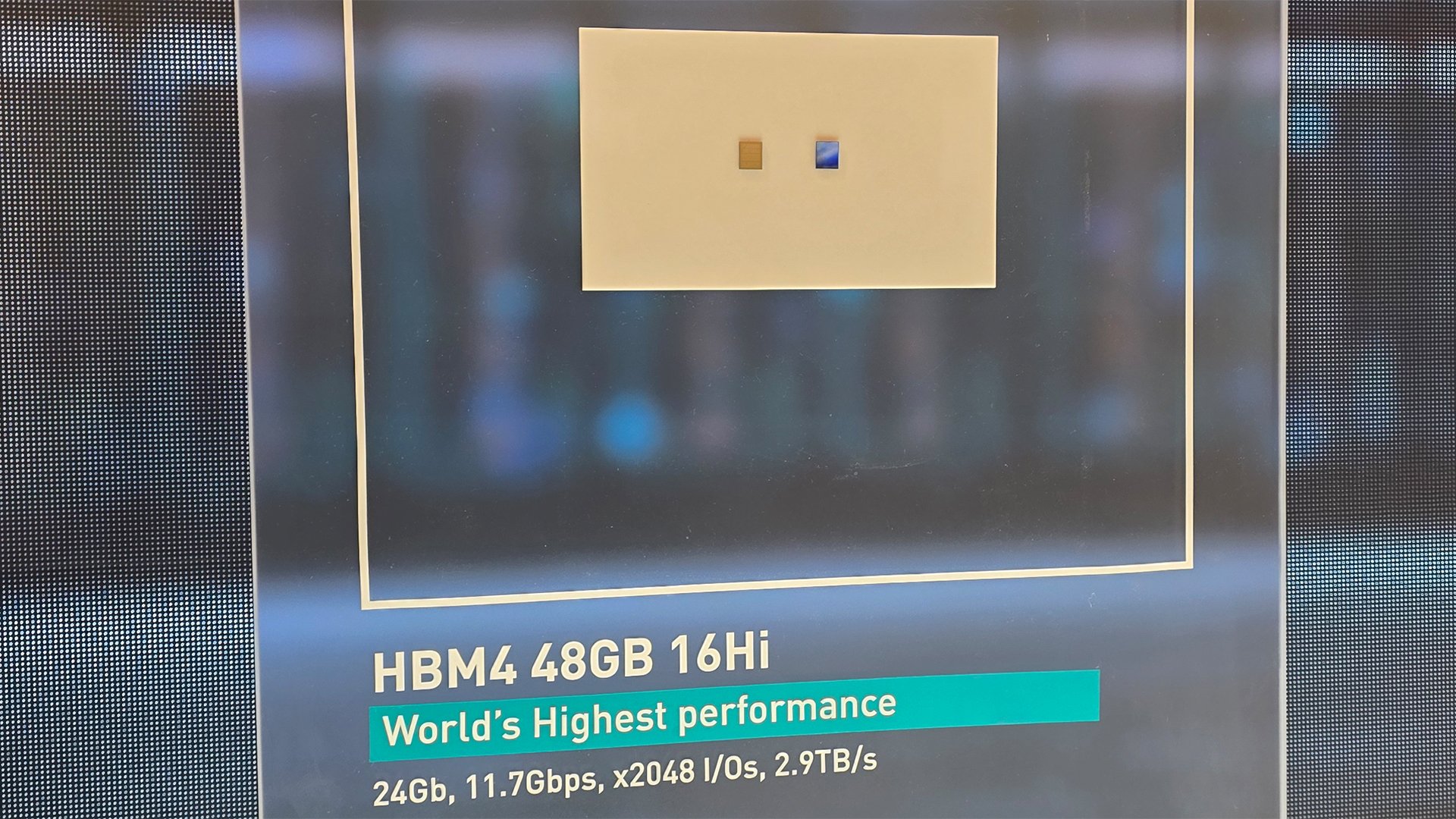
SK Hynix unveiled the industry's first 16-layer HBM4 memory stack at CES, delivering 48GB capacity and 10 GT/s speeds over a 2,048-bit interface to power future AI accelerators.

SK Hynix has publicly demonstrated its 16-layer (16-Hi) HBM4 memory stack for the first time, marking a significant leap in high-bandwidth memory technology for AI accelerators. The prototype, showcased at CES, delivers 48GB capacity per stack with data transfer speeds reaching 10 gigatransfers per second (GT/s) across a 2,048-bit interface. This represents a 25% speed increase over JEDEC's baseline HBM4 specification and directly addresses hyperscaler demands for higher bandwidth efficiency in large-scale AI deployments.
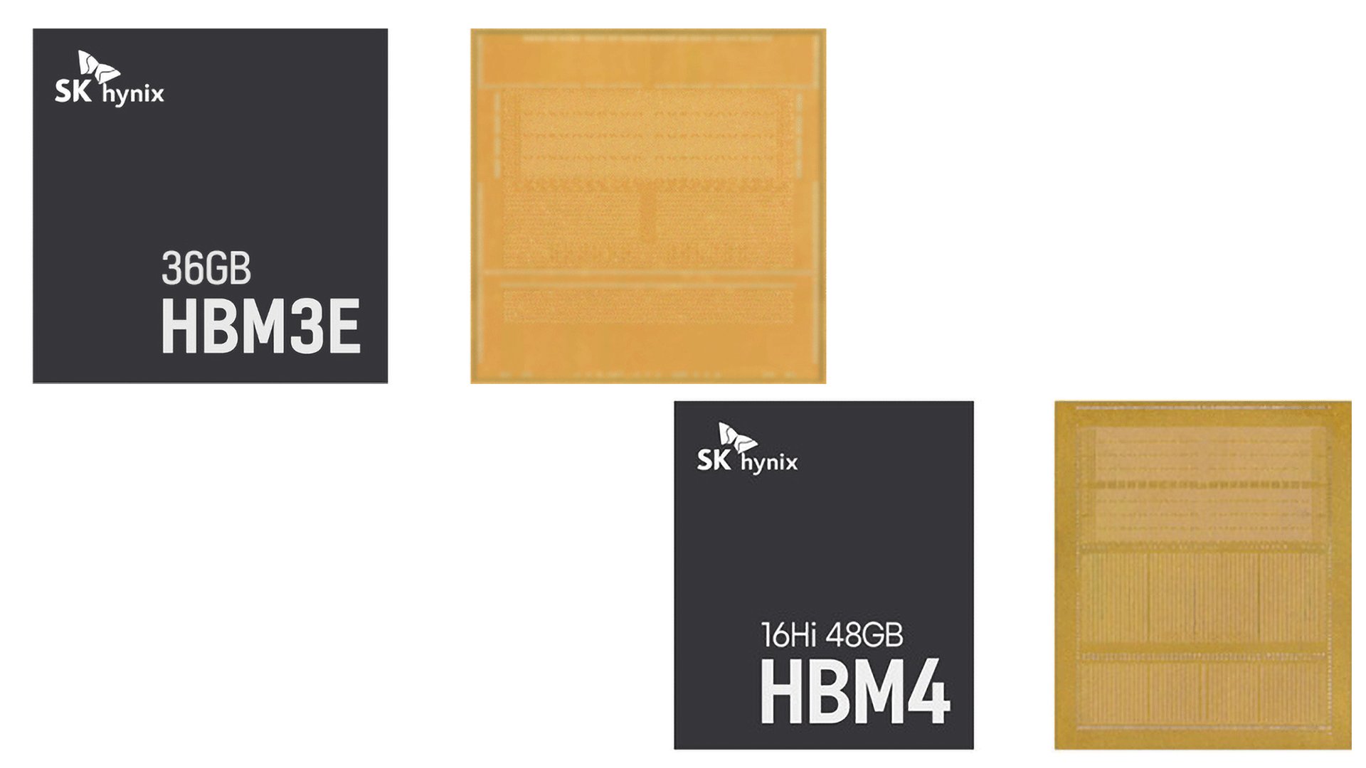 Image: HBM3E vs HBM4 comparison (Credit: SK Hynix)
Technical Specifications and Packaging Innovations
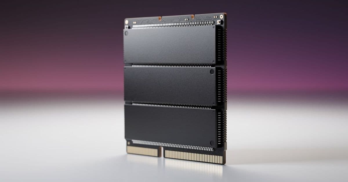
HBM4 maintains the same physical footprint as current HBM3E modules (~10.5 × 12.0 mm) but extends stack height to ~950µm for 16-layer configurations versus ~750µm for 12-layer HBM3E. The expanded layer count enables higher density while accommodating HBM4's doubled interface width (2,048-bit vs. HBM3E's 1,024-bit). SK Hynix attributes this density achievement to its proprietary MR-MUF (Mass Reflow Molded Underfill) packaging technology. This process mounts multiple DRAM dies on a base substrate in a single reflow step, then fills gaps between layers with mold material for structural integrity and thermal management.
Backside pin analysis reveals critical design differences: HBM4 exhibits a denser, more uniform bump layout across its entire substrate compared to HBM3E's segmented arrangement. This redistributes power delivery and ground contacts to support the interface's doubled signal count and higher power requirements. While HBM3E shows visible separation between I/O and power zones, HBM4 integrates these elements cohesively—a design necessity for maintaining signal integrity at 10 GT/s speeds.
Performance and Manufacturing Advantages
The 10 GT/s operational speed demonstrated by SK Hynix exceeds JEDEC's 8 GT/s standard, providing headroom for AI chipmakers like Nvidia to optimize power efficiency in hyperscale deployments. Each stack's 48GB capacity (3GB per die) is manufactured using SK Hynix's fifth-generation 1b-nm (10nm-class) process, balancing high yields with improved transistor density. The mature node reduces defect rates compared to newer processes, potentially lowering production costs—though end-user pricing remains influenced by packaging complexity and testing overhead.
Market Impact for AI Infrastructure
This advancement directly targets next-generation AI accelerators requiring memory bandwidth beyond HBM3E's limits. The 2,048-bit interface doubles theoretical peak bandwidth to 2.05 TB/s per stack (calculated as 2,048 bits × 10 GT/s ÷ 8 bits/byte). For context, Nvidia's current H200 GPU uses eight HBM3E stacks totaling 141 GB/s memory bandwidth; equivalent HBM4 configurations could approach 300 GB/s. This scaling enables larger AI model parameters to reside entirely in GPU memory, reducing latency-critical data fetches from slower storage.
Industry adoption timelines remain fluid, with SK Hynix planning volume production around 2026. The technology's compatibility with existing footprints eases integration into accelerator designs, while MR-MUF packaging provides thermal headroom for sustained high-speed operation. As hyperscalers like Google and Microsoft push AI model complexity, HBM4's bandwidth-density combination positions it as a foundational technology for trillion-parameter-scale training clusters. For detailed specifications, refer to SK Hynix's HBM product portfolio and JEDEC's HBM standardization documents.
 Image: Anton Shilov, Contributing Writer
Comments
Please log in or register to join the discussion