
Neurophos unveils optical processing unit with radically miniaturized photonic components promising 10x higher AI performance than Nvidia Rubin at equivalent power.
Neurophos, an Austin-based AI chip startup backed by Bill Gates' Gates Frontier Fund, has developed an optical processing unit (OPU) featuring optical transistors approximately 10,000 times smaller than current silicon photonics components. This breakthrough enables a single photonic sensor measuring 1,000 by 1,000 elements—15 times larger than the 256x256 matrices common in AI GPUs—while operating at unprecedented 56 GHz clock speeds.
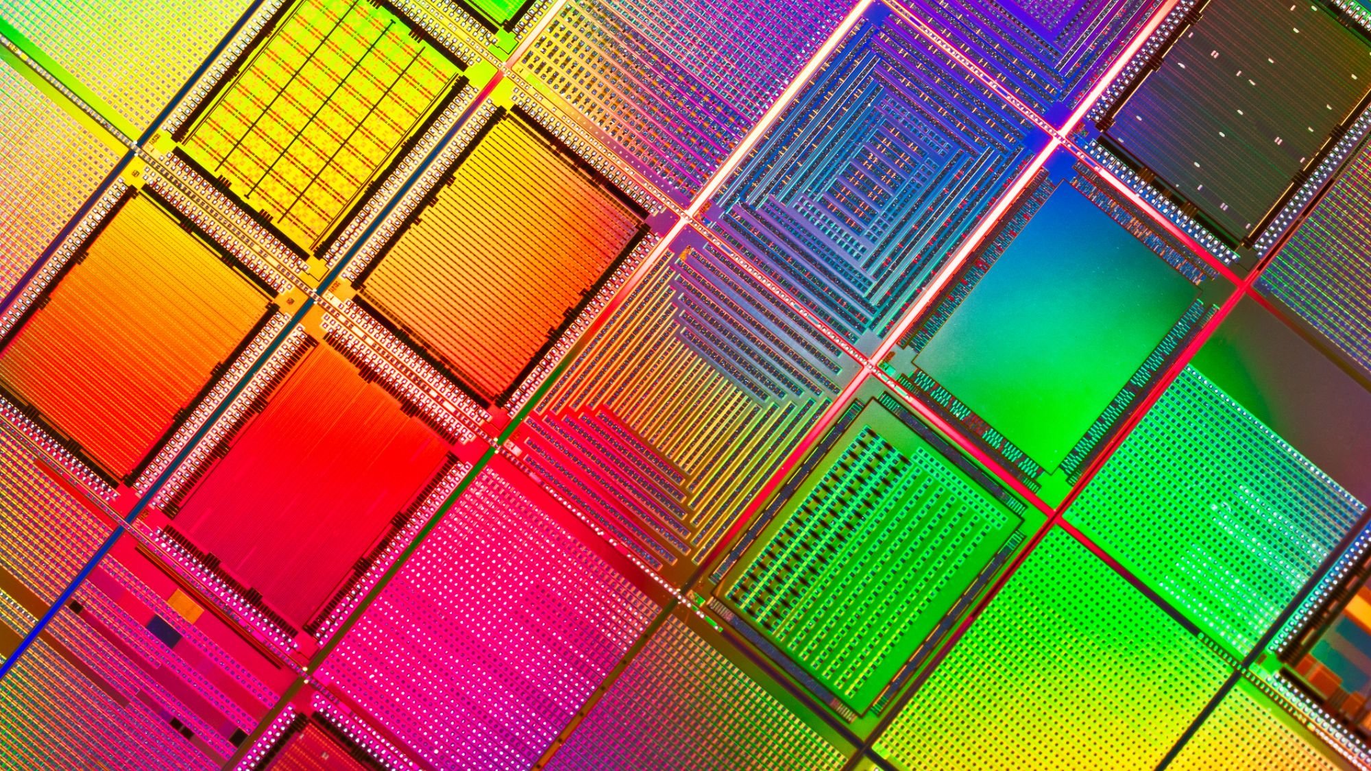
The company's Tulkas T100 OPU prototype demonstrates radical miniaturization of photonic components. Current silicon photonics transistors measure around 2mm in length, severely limiting computational density. "You can't fit enough of them on a chip to compete with digital CMOS," explained Neurophos CEO Patrick Bowen. By contrast, Neurophos' approach shrinks optical components to scales compatible with conventional semiconductor manufacturing, potentially enabling production at fabs like TSMC or Intel.

Performance projections indicate the optical accelerator could deliver ten times the computational throughput of Nvidia's upcoming Vera Rubin NVL72 AI supercomputer in FP4/INT4 workloads while maintaining similar power consumption. This efficiency stems from three architectural advantages: the massive 1,000x1,000 matrix tile size enabling parallel operations, photonic processing eliminating electron resistance heat, and the 56 GHz operating frequency—six times faster than Nvidia's current GPU boost clocks and over six times Intel's desktop processor frequency record.
Despite having the optical equivalent of just one tensor core versus Rubin's reported 576 cores, the T100 leverages photonic parallelism differently. The design concentrates computational density within specialized optical matrices rather than replicating numerous digital cores. Neurophos plans to integrate these photonic engines with conventional CMOS dies handling memory and control functions.
Manufacturing readiness remains the critical path. While compatible with existing semiconductor processes, volume production isn't projected until 2028. Key challenges include integrating sufficient SRAM buffers and vector processing units to feed the optical matrix at required data rates. The photonic approach also requires novel packaging to manage light sources and thermal conditions.

Silicon photonics represents a strategic frontier for AI acceleration, with Nvidia already deploying Spectrum-X photonic networking in Rubin platforms and AMD establishing a $280 million silicon photonics research hub. Neurophos' transistor miniaturization breakthrough potentially accelerates optical computing's viability for mainstream AI workloads, though technical and manufacturing hurdles remain before 2028's targeted production timeline.
Jowi Morales is a technology journalist specializing in semiconductor architectures and AI hardware.
Comments
Please log in or register to join the discussion