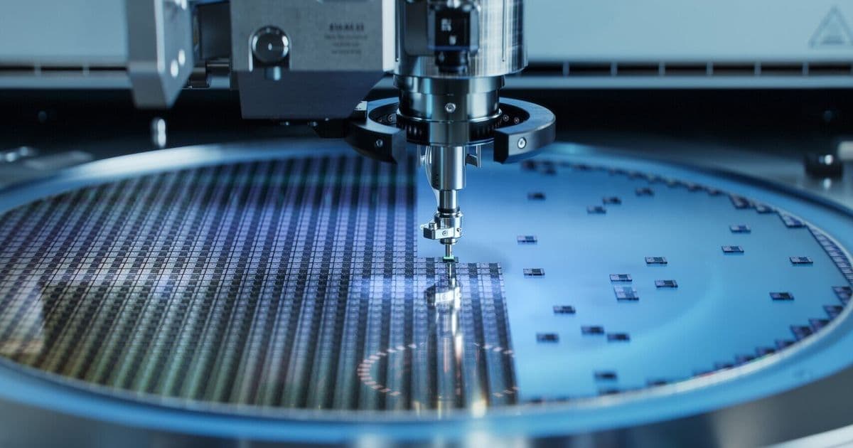
Chinese semiconductor giant SMIC has successfully achieved volume production of a 5nm-class node using only deep ultraviolet (DUV) lithography, bypassing the need for extreme ultraviolet (EUV) tools. This breakthrough, confirmed by TechInsights in the Huawei Kirin 9030 SoC, represents a significant step toward Chinese semiconductor independence despite facing substantial yield challenges.
Breaking Barriers: SMIC Achieves 5nm Node Production Without EUV Lithography
Chinese semiconductor giant SMIC has successfully achieved volume production of a 5nm-class node using only deep ultraviolet (DUV) lithography, bypassing the need for extreme ultraviolet (EUV) tools. This breakthrough, confirmed by TechInsights in the Huawei Kirin 9030 SoC, represents a significant step toward Chinese semiconductor independence despite facing substantial yield challenges.
A Technical Triumph Against Geopolitical Odds
In a development that underscores both technical ingenuity and geopolitical determination, Semiconductor Manufacturing International Corporation (SMIC) has officially announced volume production of its N+3 node, classified as 5nm-class. This achievement marks China's most advanced semiconductor node produced without any extreme ultraviolet (EUV) lithography tools, relying instead on the more accessible deep ultraviolet (DUV) technology to manufacture its silicon.
The significance of this milestone cannot be overstated. As TechInsights confirmed through analysis of the Huawei Kirin 9030 SoC, the chip has indeed been manufactured using this advanced node. This represents a full generation leap forward from SMIC's previous N+2 node, a 7nm-class technology that Huawei has utilized for its Ascend series of AI accelerators and other infrastructure components.
The DUV-EUV Divide: Physics and Engineering Challenges
At the heart of SMIC's achievement lies a fundamental challenge in semiconductor physics: the wavelength of light used in lithography directly limits the minimum feature size that can be printed on a silicon wafer. For printing smaller nodes, EUV scanners offer more possibilities due to their much smaller wavelength of 13.5 nm, compared to the smallest DUV immersion scanner wavelength of 193 nm.
This wavelength difference creates a significant technical hurdle. In a single-patterning round, the best DUV immersion scanners can achieve resolutions for nodes with sub-38 nm prints. SMIC has likely optimized these machines to reach closer to 35 nm in a single print, using multiple rounds of printing to fully etch the design.
The solution to this challenge lies in advanced multi-patterning techniques. Methods like self-aligned quadruple patterning (SAQP) have been employed in semiconductor nodes for years, allowing manufacturers to print features smaller than the wavelength of light used. It is logical that SMIC has employed similar techniques with its new N+3 node, though the implementation details remain proprietary.
However, these techniques come at a cost—both literally and figuratively. Each additional patterning step increases manufacturing time, complexity, and the chance of defects. This is where SMIC faces its most significant challenge: yield.
The Yield Conundrum: Economic Viability at Scale
Despite achieving an impressive DUV multi-patterning implementation, SMIC's N+3 node encounters significant yield challenges, particularly due to the aggressively scaled metal pitch. TechInsights analysis suggests that the Huawei Kirin 9030 SoC is likely produced at an operating loss, with a significant portion of dies being discarded or used for downgraded chips.
This yield problem creates a fundamental economic challenge. While technically feasible, producing 5nm-class chips using DUV lithography may be economically unsustainable at scale. The increased number of patterning steps, longer processing times, and higher defect rates all contribute to a cost structure that cannot compete with nodes produced using EUV lithography.
The industry standard for economically viable manufacturing typically requires yields above 80% for mature processes. Given the technical challenges faced by SMIC, it's reasonable to assume current yields fall significantly below this threshold, though exact figures remain undisclosed.
Strategic Implications: Breaking the EUV Monopoly
The achievement takes on added significance when viewed through the lens of geopolitical tensions in the semiconductor industry. Access to EUV lithography technology has been restricted for Chinese manufacturers due to export controls, effectively capping their ability to produce the most advanced chips.
SMIC's breakthrough represents a strategic response to these limitations. By developing a viable 5nm-class process using DUV tools, the company has demonstrated that technological advancement can continue even when faced with equipment restrictions.
This development aligns with China's broader strategy to establish a complete domestic semiconductor supply chain. In September 2025, SMIC was testing an immersion DUV lithography scanner developed by Shanghai Yuliangsheng Technology, part of an effort to establish a local wafer fabrication equipment industry and lessen reliance on Western suppliers.
However, it's important to note that the Yuliangsheng system was described as an immersion DUV scanner intended for 28nm class processes, comparable to older Twinscan designs from around 2008. It's unlikely that SMIC has achieved a breakthrough in such a short period to adapt this technology for 5nm production. Therefore, the new SMIC N+3 node is likely made using ASML's DUV tools that were acquired before restrictions were fully implemented.
The Road Forward: From Technical Feat to Competitive Reality
While SMIC's achievement is undeniably impressive from a technical standpoint, the path to true competitiveness remains challenging. The company has demonstrated that it can produce 5nm-class chips without EUV equipment, but doing so economically at scale remains a significant hurdle.
The development also raises questions about the future of semiconductor manufacturing. Will we see a bifurcation in the industry, with different technology paths emerging in different regions? Or will the physics of semiconductor manufacturing eventually render DUV-based advanced nodes economically unviable?
For now, SMIC's achievement stands as a testament to engineering ingenuity in the face of significant technical and geopolitical constraints. It represents a crucial step in China's quest for semiconductor self-sufficiency and demonstrates that innovation can find pathways even when the most obvious routes are blocked.
As the global semiconductor landscape continues to evolve, developments like SMIC's N+3 node production will be watched closely—not just for their technical specifications, but for what they reveal about the future of technological independence in an increasingly interconnected world.
Comments
Please log in or register to join the discussion