A tech teardown specialist's extreme methods reveal the Xeon Silver 4110 silicon die through unconventional delidding, highlighting both the accessibility and limitations of reverse engineering modern processors.
The semiconductor industry's fascination with reverse engineering processor dies received an unconventional update this week as tech channel Hackinator demonstrated a radical approach to CPU teardown. Using a blowtorch, hunting knife, and wood chopping block, the channel successfully exposed the silicon patterns of an Intel Xeon Silver 4110 processor, albeit through methods that would make traditional semiconductor engineers cringe.
The Xeon Silver 4110: A Mid-Range Enterprise Processor
The Intel Xeon Silver 4110 represents Intel's entry-level server processor lineup, built on the 14nm++ process node with a TDP of 85W. This 8-core, 16-thread processor operates at base frequencies of 2.1GHz, with a maximum turbo frequency of 3.7GHz. The processor features 11MB of L3 cache and supports up to 768GB of DDR4-2666 memory across 12 DIMM slots. Despite being positioned as Intel's most affordable Xeon Scalable processor, the 4110 remains a significant component in data center infrastructure, particularly for small to medium business workloads.
Delidding Process: From Standard to Extreme
Traditional CPU delidding typically involves careful heating with a heat gun or hot plate to soften the thermal interface material (TIM) between the integrated heat spreader (IHS) and the CPU die. Specialized tools like delidding kits or thin guitar strings are then used to separate the components. This process, while risky, is often performed to replace TIM with higher-performance alternatives for better thermal management.
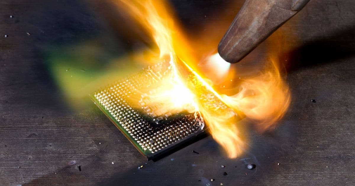
Hackinator's approach diverges dramatically from industry standards. The process begins by mounting the Xeon Silver 4110 to a wood chopping block using washers and screws, effectively creating a makeshift vise. A hot air soldering gun, mounted on a tripod, heats the IHS to approximately 200-250°C—the temperature required to soften the solder bond between the IHS and the substrate. This step is critical, as Intel uses fluxless solder in their enterprise processors, which requires higher temperatures than the TIM used in consumer CPUs.
The 'Hackinator' Methodology
What follows represents perhaps the most aggressive delidding approach documented in the public domain. Using a Gerber hunting knife and flat-edged screwdriver, the channel applies significant mechanical force to pry the IHS from the substrate. This brute-force approach would typically result in die damage in conventional delidding, but the Xeon's substrate construction provides some resilience.
With the IHS removed, the channel adds a metal frame and reapplies grip screws to the substrate before applying more heat. The substrate—composed primarily of organic materials with embedded interconnects—is then subjected to direct flame from a blowtorch. This step incinerates the organic substrate material, leaving behind the silicon die and its surrounding packaging.
The liberated die, now covered in soot and residue, undergoes cleaning with a chemical spray and toothbrush before an etching paste is applied. This paste removes the protective layer over the silicon die, revealing the underlying circuit patterns. While conventional die preparation involves precise chemical etching and polishing, Hackinator's method achieves comparable results through aggressive mechanical and thermal means.
Technical Analysis and Implications
The Xeon Silver 4110 die, measuring approximately 12mm × 12mm, contains approximately 2.2 billion transistors arranged in Intel's 14nm++ process technology. The die's layout reveals Intel's standard core complex arrangement, with eight processor cores organized into two CCX (Core Complex) units, each containing four cores. The die also includes the uncore components: L3 cache, memory controller, and system agent.
The reverse engineering process reveals several interesting aspects of Intel's packaging approach:
Solder Bond Quality: The Xeon's solder bond proved more resilient than typical consumer CPUs, requiring higher temperatures and more force to separate. This reflects Intel's quality standards for enterprise processors.
Substrate Construction: The organic substrate's ability to withstand blowtorch exposure indicates the use of high-temperature materials, likely polyimide-based laminates with ceramic fillers.
Die Protection Layer: The etching paste successfully removed the passivation layer, revealing the metal interconnect layers. This layer typically consists of silicon nitride or silicon oxynitride deposited via chemical vapor deposition.
Industry Context and Reverse Engineering Trends
This extreme teardown highlights an interesting trend in semiconductor reverse engineering. While traditional methods focus on preserving die integrity for functional analysis, more aggressive approaches are emerging for purely visual inspection. The accessibility of powerful microscopes and digital imaging has made detailed die photography increasingly common, even with imperfect sample preparation.
From a supply chain perspective, the ability to visually inspect dies provides valuable information about:
- Process node characteristics (transistor density, layout patterns)
- Design implementation approaches (core arrangement, cache organization)
- Manufacturing quality (die symmetry, defect patterns)
However, the Hackinator method's destructive nature limits its utility for functional analysis. Unlike focused ion beam (FIB) preparation or chemical etching, thermal and mechanical damage prevents electrical testing of the exposed die.
Market Implications and Future Directions
The extreme delidding demonstration, while entertaining, underscores broader industry challenges:
Accessibility of Analysis: As semiconductor processes advance beyond 7nm, traditional reverse engineering becomes increasingly difficult. The Xeon Silver 4110's 14nm++ node represents a relatively mature technology where physical analysis remains feasible.
Thermal Management Evolution: The aggressive delidding approach reflects the ongoing battle against thermal constraints in computing. As processors continue to increase in transistor count, thermal interface materials and packaging become critical performance differentiators.
Educational Value: Despite its unconventional methods, the teardown provides valuable educational content about processor construction, helping demystify the complex engineering that goes into modern CPUs.
As semiconductor manufacturing continues to advance, the balance between preservation and destruction in reverse engineering will remain an interesting technical and ethical consideration. While Hackinator's methods may never become standard practice, they demonstrate the lengths to which enthusiasts will go to satisfy curiosity about the silicon that powers our digital world.
For those interested in more conventional CPU teardowns, Intel offers technical documentation on their packaging processes, while companies like TechInsights provide professional reverse engineering services that maintain die functionality while revealing internal structures.
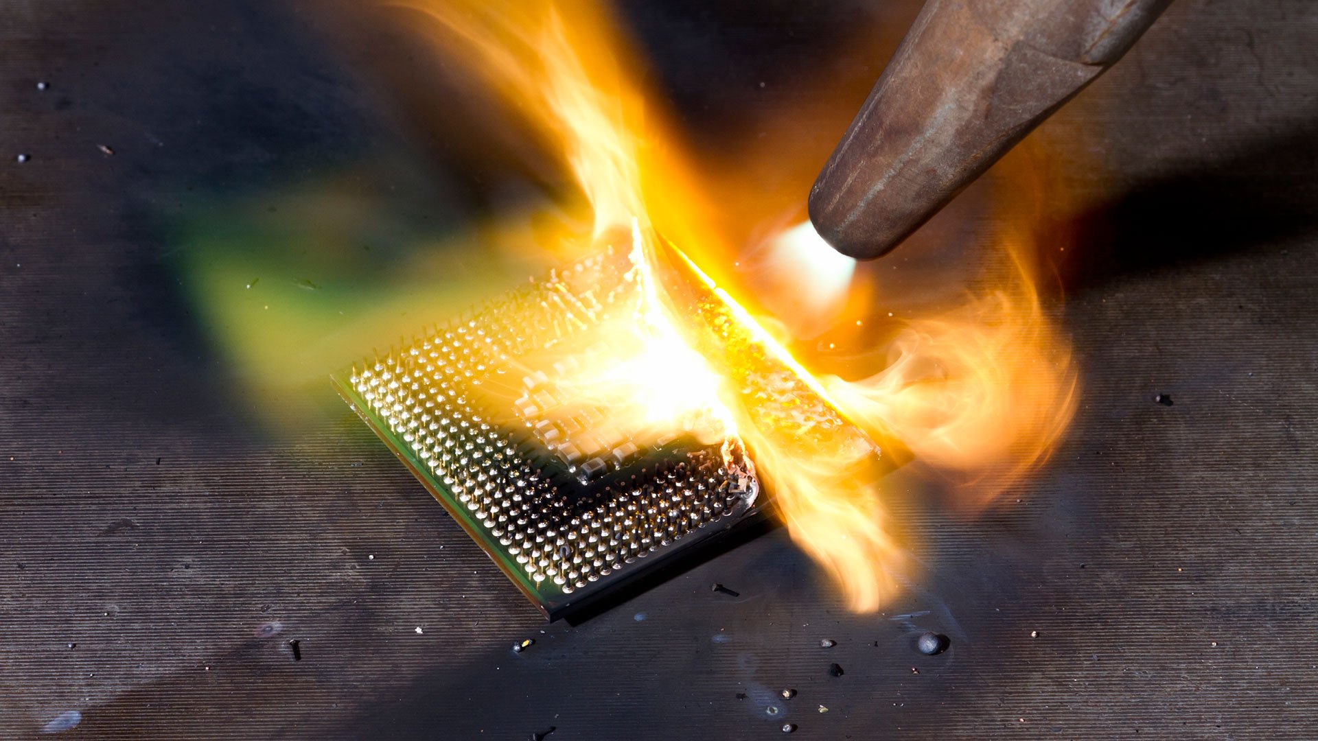
The Xeon Silver 4110 undergoes extreme delidding treatment. While unconventional, this approach reveals details of Intel's enterprise processor construction that would remain hidden with more conservative methods.
Comments
Please log in or register to join the discussion