Reiner Pope walks through the low‑level building blocks of AI accelerators, from AND gates to full‑adders, then shows how data‑movement costs drive the shift from scalar cores to systolic arrays. The talk clarifies why multiply‑accumulate (MAC) units dominate chip area, why precision scaling is quadratic, and what practical trade‑offs (register‑file size, clock speed, ASIC vs FPGA) still limit real‑world performance.
What’s claimed in the lecture
- AI chips are essentially large collections of multiply‑accumulate (MAC) units built from basic logic gates.
- Using lower‑precision formats (FP4, FP8) gives a quadratic reduction in area, so halving the bit‑width more than doubles throughput.
- The dominant cost in a classic CUDA core is the mux‑based register‑file read/write path, not the MAC itself.
- Systolic arrays (the “Tensor Core” idea) solve this by keeping the weight matrix on‑chip and moving only vectors, dramatically reducing data‑movement overhead.
- Design decisions boil down to sizing the systolic array vs. the register file, clock‑frequency vs. pipeline depth, and whether to invest in an ASIC or an FPGA.
What’s actually new or noteworthy
- Concrete gate‑level accounting – Pope counts AND gates for partial‑product generation and full‑adders for reduction, arriving at a simple formula: a p‑bit × q‑bit MAC needs p·q ANDs and p·q full‑adders. This matches textbook multiplier analysis but is rarely spelled out in product briefs.
- Mux cost dominance – The lecture shows that an 8‑entry, p‑bit register file requires
3 × n × pAND gates just to select three operands for a MAC. For a 4‑bit MAC (p=4) that’s 96 AND gates, dwarfing the 16 ANDs needed for the actual multiplication. The point is not new, but the explicit gate‑count comparison is a useful sanity check for architects who see only high‑level performance numbers. - Quadratic precision scaling – The claim that FP4 is three times faster than FP8 on recent Nvidia GPUs (B300+) reflects the fact that area scales with the square of bit‑width, not linearly. This nuance explains why vendors now quote “3× FP4 vs FP8” instead of the older “2×” rule of thumb.
- Systolic array as a data‑movement optimizer – By storing the weight matrix locally, the array reduces the register‑file bandwidth requirement from x·y to x (where x is the vector dimension). The lecture’s description of feeding the matrix slowly (one element per cycle) while reusing it for many vectors is a practical implementation detail that many high‑level overviews skip.
- Pipeline register trade‑off – Pope emphasizes that adding registers to meet a tighter clock can inflate area because each register costs roughly one gate‑equivalent. The sweet spot is often a modest pipeline depth that keeps the critical path under the target clock while preserving compute density.
- FPGA vs. ASIC cost model – The talk reiterates the classic rule: an FPGA’s lookup table (LUT) implements a 4‑input truth table using a 16‑to‑1 mux, costing roughly 32 primitive gates. An ASIC implements the same function with a handful of gates, explaining the order‑of‑magnitude power and area advantage of ASICs.
Limitations and practical considerations
- Precision flexibility is not free – While the area for FP4 vs. FP8 MACs differs quadratically, the surrounding data‑path (register files, interconnect, memory bandwidth) often limits how many low‑precision units can be packed. A chip that doubles FP4 MAC density may still be bottlenecked by off‑chip memory.
- Systolic array size vs. latency – Larger arrays amortize register‑file costs but increase the distance data must travel between the vector unit and the matrix unit. This can raise energy per operation and limit scaling beyond a certain array dimension.
- Clock‑speed ceiling – The lecture notes that modern processes allow roughly 10‑30 primitive gates per clock cycle. Pushing beyond ~3 GHz typically forces designers to insert many pipeline registers, which reduces the effective compute per cycle and can hurt overall throughput.
- FPGA re‑configurability vs. ASIC efficiency – FPGAs excel when workloads change frequently, but the 10× area and power penalty means they are rarely competitive for the massive inference workloads that dominate today’s data‑center AI traffic.
- Branch prediction and deterministic latency – Pope points out that CPUs sacrifice deterministic timing for aggressive speculation. Even AI chips that claim deterministic latency (e.g., Groq, TPU) still rely on predictable memory access patterns; any irregular sparsity or control flow can re‑introduce latency variance.
- Biological analogy limits – Comparing silicon systolic arrays to the brain’s unstructured connectivity is useful for intuition but can be misleading. Neuronal communication is analog, massively parallel, and operates at millisecond timescales, whereas silicon logic is binary, clocked, and optimized for gigahertz operation. Energy per operation on a chip is dominated by charging/discharging capacitances, a factor that does not map cleanly to metabolic energy in neurons.
Takeaway for practitioners
- When evaluating a new AI accelerator, look beyond the headline FLOP count. Verify the gate‑level area breakdown (MAC vs. register‑file vs. interconnect) to understand where performance gains actually come from.
- Precision scaling is more than a linear speed‑up; expect super‑linear area reductions, but also verify that memory bandwidth and on‑chip scratchpad sizes can keep up.
- Systolic arrays are not a silver bullet. Their efficiency hinges on the ability to keep weight matrices resident on‑chip and on the vector‑to‑matrix bandwidth. Designs that expose a splittable systolic array (as MatX hints) aim to balance flexibility with the low‑movement advantage.
- For low‑latency, high‑throughput workloads that rarely change, an ASIC with a well‑sized systolic array will dominate an FPGA despite the latter’s programmability.
- Finally, remember that clock frequency is a lever, not a goal. Pushing the clock without proportionally increasing compute per cycle can waste silicon and power.

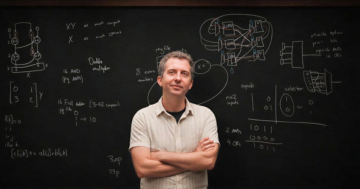
Figure: Reiner Pope’s blackboard sketch of a 4‑bit × 4‑bit MAC built from AND gates and full‑adders.
Comments
Please log in or register to join the discussion