
Startup Taalas has developed a custom ASIC chip that runs Llama 3.1 8B at 17,000 tokens per second by physically etching model weights onto silicon, eliminating GPU memory bottlenecks.
Taalas, a 2.5-year-old semiconductor startup, has unveiled an ASIC chip capable of running Meta's Llama 3.1 8B model at 17,000 tokens per second using 3/6-bit quantization. This performance equates to generating approximately 30 pages of A4 text per second while consuming 90% less power than GPU-based systems at one-tenth the ownership cost.
The GPU Bottleneck Problem
Current GPU-based inference faces fundamental limitations. Large language models like Llama 3.1 8B contain 32 sequential layers. During token generation:
- The GPU fetches layer weights from external VRAM/HBM
- Computes matrix multiplications
- Stores intermediate activations back to memory
- Repeats for all 32 layers
- Restarts the entire process for each new token
This constant data shuffling creates a memory bandwidth bottleneck known as the Von Neumann bottleneck, where energy and latency are dominated by data movement rather than computation.
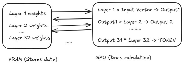 GPU inference requires repeated memory access for each layer computation
Taalas' Silicon Solution
Taalas bypasses this bottleneck by physically etching Llama's 32-layer architecture directly onto silicon. Model weights become physical transistor configurations rather than stored parameters. Their approach features:
- Hardwired model: Weights permanently encoded in chip transistors
- Pipelined data flow: Intermediate results pass directly to next layer via physical wiring
- 4-bit multiplier: Proprietary transistor design handling 4-bit operations efficiently
When input embeddings enter the chip, signals propagate through the transistor layers like water through pipes, with computations occurring during transit. This eliminates weight-fetching and intermediate storage for activations.
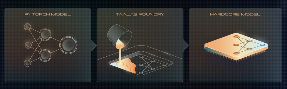 Taalas' architecture embeds model weights directly into silicon pathways
Memory and Manufacturing Innovations
The chip uses minimal on-chip SRAM exclusively for:
- KV cache maintenance
- LoRA adapter storage
This avoids external DRAM entirely, sidestepping both bandwidth limitations and DRAM supply constraints. For manufacturing scalability, Taalas created:
- Base chip with generic transistor grid
- Customizable top metal layers
This reduces chip adaptation time from years to approximately two months per model. While slower than software iterations, this represents unprecedented agility for custom silicon.
Implications
By eliminating memory bottlenecks, Taalas achieves:
- 10x speed increase vs. top GPU inference systems
- 90% power reduction per token
- 90% cost reduction in total ownership
The approach could enable real-time LLM applications previously hindered by latency and cost barriers. As Taalas moves toward production, their wafer-scale integration method may redefine efficiency boundaries for specialized AI hardware.
Images sourced from Taalas technical blog
Comments
Please log in or register to join the discussion