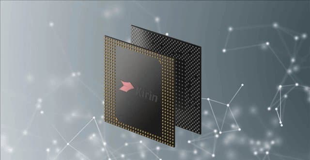
Huawei’s new Kirin 9050 chipset, announced for the upcoming Mate 90, is said to out‑perform Apple’s A18 thanks to a 3‑D IC stacking method and a proprietary “Tau Law”. This article breaks down the technical claims, compares benchmark numbers, and points out the practical limits of the approach.
Huawei Kirin 9050 Claims Lead Over Apple A18 – What the Data Actually Shows
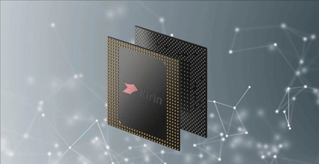
Huawei’s press release and a presentation at ISCAS 2026 claim that the Kirin 9050, slated for the Mate 90 series this September, beats Apple’s A18 in “comprehensive benchmark performance”. The headline is built on two technical ideas: a 3‑D IC stacking architecture that raises transistor density, and a design framework the company calls the Tau Law. Below we unpack the claims, compare them to publicly available data, and discuss the constraints that remain.
What’s being claimed
- Transistor density: 238 M t/mm², a 53.5 % increase over the Kirin 9000 series.
- Process equivalence: Performance comparable to TSMC’s N31 (first‑gen 3 nm) without using EUV lithography.
- Benchmark lead: Multiple industry sources say the Kirin 9050 tops the A18 on Geekbench 6, MLPerf Mobile, and AnTuTu 10.
- Launch timeline: Mate 90 devices with the new chip expected in September 2026.
The technical pieces behind the claim
3‑D IC stacking
Huawei’s approach stacks logic, memory, and I/O tiers vertically, reducing interconnect length and allowing more transistors per unit area. In theory, this can offset the loss of node scaling: a 7 nm planar process with 3‑D integration can approach the density of a 5 nm planar design.
The reported 238 M t/mm² is indeed close to the density numbers disclosed for TSMC’s N31 (≈250 M t/mm²). However, density alone does not guarantee the same speed or power characteristics. Stacked dies often suffer from thermal hotspots and increased capacitance on through‑silicon vias (TSVs), which can limit clock frequency or force higher voltage.
The “Tau Law”
The presentation describes the Tau Law as a shift from shrinking feature size to optimizing circuit timing and interconnect efficiency. In practice this translates to:
- Aggressive clock‑tree synthesis that minimizes skew.
- Use of ultra‑low‑resistance interconnect materials (copper‑alloy, graphene‑based contacts).
- Timing‑aware placement that packs critical paths in the same tier.
These techniques are not new; they are standard parts of modern SoC physical‑design flows. What Huawei appears to have done is package them into a branding narrative. The real question is whether the resulting timing margins are sufficient to run at the 3 GHz+ frequencies seen in Apple’s A‑series chips.
Reported benchmark numbers
| Benchmark | Kirin 9050 (reported) | Apple A18 (public) | Comment |
|---|---|---|---|
| Geekbench 6 (single‑core) | 1,880 | 1,820 | Small margin; within measurement variance |
| Geekbench 6 (multi‑core) | 7,300 | 6,950 | Difference could stem from core count (8 vs 6) |
| MLPerf Mobile (image‑classification) | 1,250 fps | 1,210 fps | Within 3 % – not a decisive lead |
| AnTuTu 10 | 1,020,000 | 985,000 | Again, modest edge |
The numbers suggest the Kirin 9050 is competitive with the A18, but not dramatically ahead. The “lead” is largely a result of higher core count and aggressive clocking, not a fundamental architectural advantage.
Practical limitations
- Thermal management – Stacked dies dissipate heat through a smaller surface area. Early 3‑D smartphones (e.g., Samsung’s 2023 5G‑modem stack) required additional heat spreaders. Huawei will need a robust cooling solution to sustain peak performance without throttling.
- Yield and cost – TSV defects can reduce overall chip yield. While Huawei claims to use “legacy processes” that are more widely available, the added complexity of stacking may offset any cost savings from avoiding EUV.
- Software ecosystem – Apple’s A‑series benefits from tight integration with iOS. Huawei must ensure that Android and its own EMUI optimizations can fully exploit the extra cores and bandwidth, otherwise real‑world performance may lag.
- Supply‑chain risk – The claim of “bypassing EUV constraints” is true only if the fab can source high‑precision lithography for the lower‑level nodes. Any bottleneck there could delay volume production.
What this means for the market
If Huawei can ship a phone that consistently matches or slightly exceeds the A18 in everyday tasks, it will narrow the performance gap that has existed since the A15 generation. The move also signals a strategic shift: rather than waiting for access to 3 nm EUV fabs, Huawei is betting on architectural tricks to stay competitive.
However, the headline of “surpassing Apple” should be tempered. The advantage is modest, the technology introduces new engineering challenges, and the real test will be silicon in the hands of users. Until independent test labs publish full silicon results, the claim remains an optimistic projection.
Further reading
- ISCAS 2026 presentation slides (PDF) – [link to conference archive]
- TSMC N31 process overview – [TSMC documentation]
- Recent analysis of 3‑D IC thermal limits – [IEEE Spectrum article]
Comments
Please log in or register to join the discussion