A detailed look at the French‑built Mitra 125 MS minicomputer that powered NASA’s Spacelab, focusing on the reverse‑engineered ALU/register board, its component chips, and the broader context of European computer history.
Inside the Spacelab Mitra 125 MS: Reverse‑Engineering a 1980‑Era ALU Board
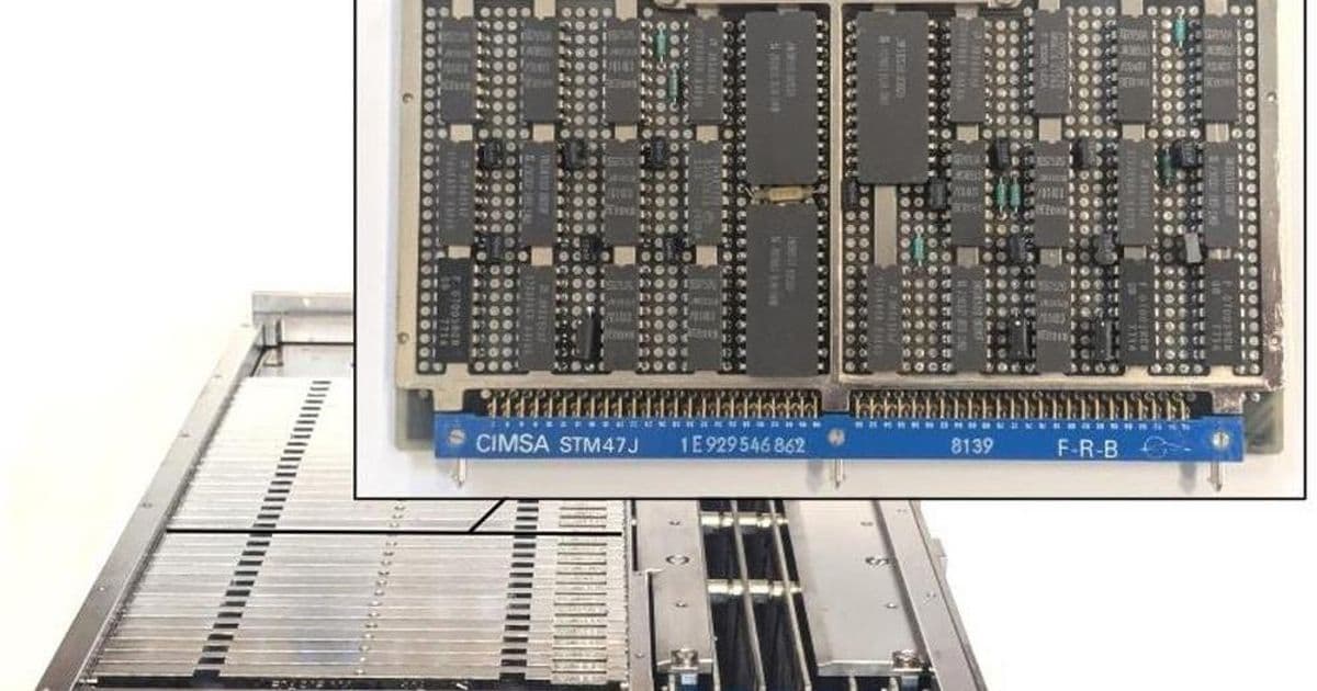
Spacelab was a pressurized laboratory that rode in the cargo bay of the Space Shuttle, giving astronauts a dedicated work‑area for experiments. The laboratory’s brain was a French‑built minicomputer – the Mitra 125 MS – a militarized variant of the Mitra 125 produced by CIMSA. Unlike today’s processors, the Mitra had no single microprocessor die; its 16‑bit CPU was assembled from dozens of discrete TTL chips on several printed‑circuit boards. This article walks through the reverse‑engineering of one of those boards, the arithmetic/logic unit (ALU) register board, and explains why the design mattered for a space‑flight computer.
The Mitra 125 MS in context
- Origins – The Mitra line began in 1971 with the Mitra 15, a 16‑bit machine built by CII (Compagnie internationale d’informatique). It used magnetic‑core memory and sold nearly 8 000 units worldwide. In 1975 CII released the Mitra 125, adding memory‑management, I/O processors and a richer instruction set. CIMSA, a Thomson‑CSF subsidiary focused on military and aerospace electronics, produced the Mitra 125 MS ("militarized" and "space‑qualified") for Spacelab.
- Role on Spacelab – Each Spacelab flight carried three Mitra computers: a Subsystem Computer (controls the lab), an Experiment Computer (runs payload software), and a Backup Computer. They were mounted under the work‑bench rack inside the pressurized module, interfaced to the crew via a keyboard and a colour CRT called the Data Display System (DDS).
- Obsolescence – By the early 1990s the Mitra’s core‑memory, 128 KB capacity and 1‑2 MHz instruction rate were insufficient. In 1991 the three CIMSA machines were swapped for IBM AP‑101SL computers – essentially AP‑101S units re‑micro‑coded to execute the Mitra instruction set.
The 54S181‑based ALU board
The most complex chip on the board is the 54S181, a military‑grade version of Texas Instruments’ 74181 4‑bit ALU. Each 54S181 contains about 170 bipolar transistors and implements the full set of 4‑bit logical and arithmetic operations (AND, OR, XOR, addition, subtraction, increment, decrement, etc.). The Spacelab CPU used eight of these chips to build a 32‑bit adder, even though the processor itself was 16‑bit. The extra width sped up multiplication and floating‑point operations, which produce 32‑bit results.
Board composition
| Component | Quantity | Function |
|---|---|---|
| 54S181 ALU chips | 3 (on this board) | 4‑bit slices of the 32‑bit ALU |
| 54S182 carry‑look‑ahead | 2 (on other boards) | Fast carry generation for the 32‑bit adder |
| 54S04 hex inverters | 3 | Signal polarity conversion |
| 54S20 4‑input NAND | 1 | Basic gating for control logic |
| 54S194 4‑bit shift registers | 3 (one per register) | Implements the three 32‑bit registers (A, B, C) |
| 54LS175 quad flip‑flops | 1 | Latches intermediate data |
| 54S181‑type multiplexers (dual 4‑to‑1) | 12 on this board | Selects which of four possible sources feed each ALU input bit |
The board under study implements 12 of the 32 bits of the full ALU/register set. Each 4‑bit slice consists of one ALU chip, two multiplexers for the A inputs, two multiplexers for the B inputs, and the associated register slice.
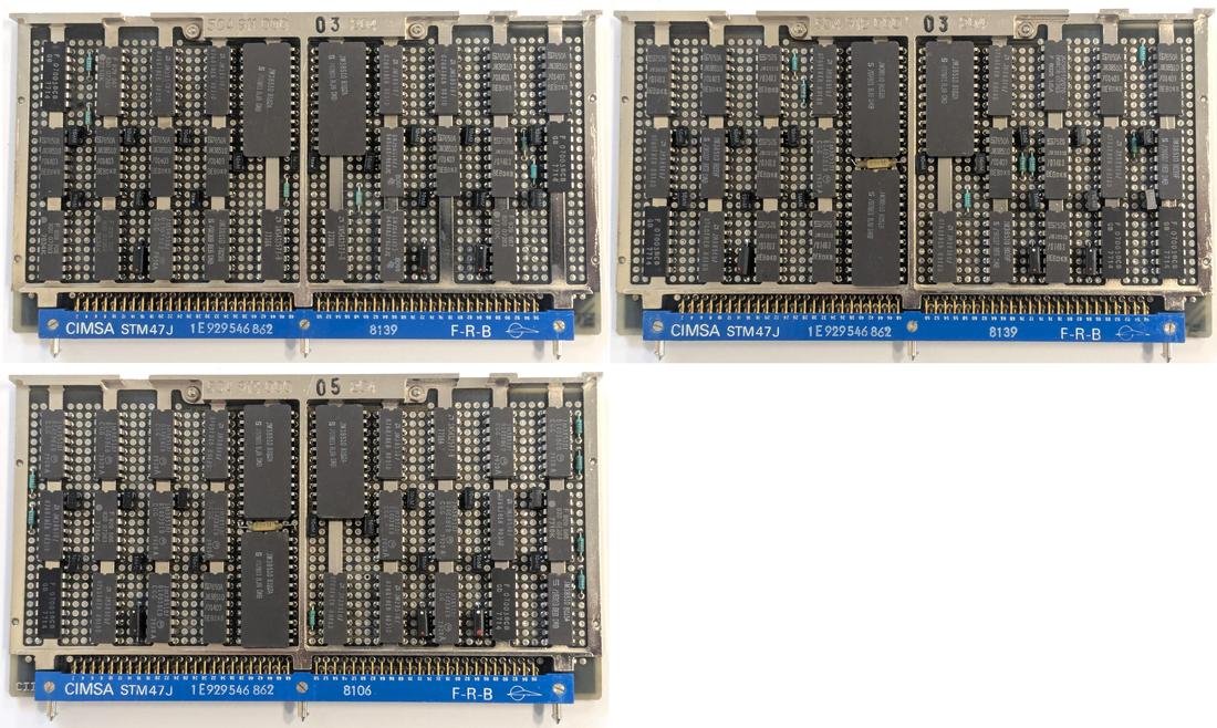
Physical quirks
- Fixed‑grid holes – Unlike modern PCBs that drill only where needed, the Spacelab boards use a regular 0.1 in grid. This style, also seen on IBM System/360 boards, simplifies automated assembly but wastes space.
- Heat‑sink bars – Metal bars run beneath each DIP package, acting as passive heat sinks for the power‑hungry bipolar chips.
- Yellow “bodge” wires – Hand‑soldered jumper wires correct routing errors; they were likely added during pre‑flight testing.
- Keyed 96‑pin connector – Three cylindrical pins with unique orientations prevent a board from being inserted into the wrong slot. The pin numbering is non‑linear (e.g., pin 52 appears between pins 49 and 51), a common practice to discourage accidental mis‑wiring.

How the ALU works in the Mitra
The 32‑bit ALU sits in the centre of the data path. Two multiplexers select one of four possible sources for each operand (A and B). Sources include:
- The three 32‑bit registers (A, B, C)
- The system bus (values fetched from memory or other registers)
- A constant “all‑1s” value, which acts as –1 in two’s‑complement arithmetic and enables decrement operations
- A “mix” bus that carries a jumble of control and status signals used by microcode for special cases
After the ALU computes a result, microcode routes the output to one of three destinations:
- Register A – a shift register that can be shifted left or right on the next cycle (useful for multiply/divide steps)
- Register B – another shift register, often used as a temporary accumulator
- Register C – a simple flip‑flop register that holds the result for the next instruction but is not directly addressable by the rest of the system
The shift registers are wired so that a left‑shift is just a different set of wires feeding the multiplexers; the registers themselves do not shift internally. This design keeps the hardware simple while still allowing the microcode to perform the bit‑shifts required for multiplication, division, and floating‑point alignment.
Reverse‑engineering process
- Continuity testing – With the board de‑soldered and free of conformal coating, a handheld multimeter was used to “beep” between pins, mapping every trace.
- Physical schematic – The initial KiCad capture reproduced the exact physical layout (chip footprints, pin locations) to keep the mapping clear.
- Logical conversion – Symbols were swapped for logical equivalents (e.g., 54S181 → 74181) and the schematic was cleaned up, moving components to reflect functional blocks.
- Verification – Re‑probing corrected a handful of mis‑identified connections; the final schematic matches the observed behaviour when the board is powered in a test rig.
The full 36‑board schematic of the Mitra 125 MS is still out of reach, but the ALU/register board alone reveals how much hardware was needed to implement a modest 16‑bit instruction set before the microprocessor era.
Why the design mattered for space
- Radiation tolerance – Military‑grade 5400‑series TTL parts were screened for radiation hardness, a requirement for the Shuttle’s low‑Earth‑orbit environment.
- Modularity – Using many identical DIP chips allowed the design to be repaired or upgraded in the field; a faulty ALU slice could be swapped without redesigning the whole board.
- Thermal management – The metal heat‑sink bars and generous spacing helped dissipate the 2–3 W per chip that bipolar TTL generates, a crucial factor in a sealed, pressurized cabin.
- Deterministic timing – Ripple‑carry adders with optional 74182 look‑ahead gave predictable instruction timing, simplifying the real‑time control loops that managed experiment sequencing.
From Mitra to IBM
When the Shuttle’s own computers were upgraded to the AP‑101S in the early 1990s, NASA chose to keep the Mitra software stack by re‑micro‑coding the new hardware. The AP‑101S already supported a 16‑bit “1750A” instruction set for aerospace applications, so a firmware update allowed it to execute Mitra opcodes. Physically, the AP‑101SL boards are larger, use surface‑mount flat‑pack ICs and semiconductor RAM, and have a completely different I/O processor, but the functional role – controlling Spacelab’s experiments and handling telemetry – remained the same.
Takeaways
- The Mitra 125 MS illustrates the pre‑microprocessor approach of building a CPU from many simple TTL parts. A 32‑bit ALU assembled from eight 4‑bit slices was enough to give a 16‑bit machine respectable arithmetic performance.
- Heat, radiation, and modularity drove the choice of military‑grade DIP packages and generous board spacing, even though it made the system bulkier than contemporary American aerospace computers.
- The reverse‑engineering workflow – continuity testing → physical schematic → logical conversion – is a practical method for documenting legacy hardware that lacks schematics, especially when the board is still physically intact.
- Understanding these historical designs provides perspective on today’s system‑on‑chip designs: many of the same trade‑offs (speed vs. power, modularity vs. density) still shape processor architecture, only now they happen at the transistor level.
For updates on this and other retro‑hardware investigations, follow the author on Bluesky, Mastodon, or via RSS.
Comments
Please log in or register to join the discussion