Japanese chemical leader JSR is opening a photoresist fab in Yunlin County, Taiwan, slated for 2028, to co‑develop EUV materials with TSMC. The move closes the last gap among Japan’s top EUV resist suppliers, pairs with a new metal‑oxide resist line in South Korea, and aims to keep Chinese entrants at bay while shortening development cycles for AI‑driven chips.
JSR Expands EUV Photoresist Production to Taiwan
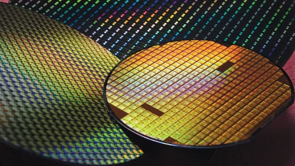
 Photoresist production line in Yunlin County, Taiwan (Image credit: TSMC)
Announcement
TSR (JSR) announced a joint venture with Taiwan’s Wah Lee Industrial and LCY Chemical to construct its first EUV photoresist fab on the island. The plant, located in Yunlin County, is targeted for commercial operation in 2028. The venture follows JSR’s recent acquisition of Inpria’s metal‑oxide resist (MOR) technology and the start‑up of a MOR line in Cheongju, South Korea.
Technical specifications
- Process focus: Conventional chemically amplified resists (CAR) for TSMC’s 2 nm‑class logic, with a long‑term shift toward tin‑oxide MOR chemistry.
- MOR advantages: Inpria data show ~5× higher EUV photon absorption than organic CARs, molecular size ~5× smaller, and etch resistance 10–100× higher. These traits reduce acid‑diffusion blur and line‑edge roughness, which become critical below 20 nm pitch.
- Capacity outlook: Exact wafer‑per‑day numbers have not been disclosed, but industry analysts estimate a mid‑size fab (≈2 k wafer per month) would satisfy TSMC’s demand for prototype and low‑volume production runs while providing a buffer for the upcoming high‑NA EUV transition.
- Co‑development model: Engineers from JSR will work side‑by‑side with TSMC process teams, eliminating the multi‑week round‑trip shipping that previously limited iteration speed. The joint venture also includes a planarization research center in Hsinchu County, co‑run with Applied Materials, to explore ALD and CVD precursor integration with the new resists.
Market implications
- Supply‑chain tightening: By locating production next to TSMC, JSR reduces logistics latency, cuts inventory holding costs, and aligns resist supply with TSMC’s aggressive AI‑chip roadmap (estimated 1.5 M‑core GPUs per year). The move mirrors the existing Taiwanese fabs of Tokyo Ohka Kogyo (TOK) and Shin‑Etsu, meaning the three Japanese EUV‑resist leaders now all have on‑site capacity.
- Competitive positioning vs. China: Japanese firms currently control ~80 % of the global photoresist market and ~85 % of EUV‑resist volume. Chinese entrants such as Hubei Dinglong and Xuzhou B&C remain below 5 % share at the ArF/EUV level. Proximity to TSMC gives JSR a timing advantage that could keep Chinese firms several development cycles behind, especially as MOR adoption expands to DRAM layers at Samsung and SK Hynix.
- Financial backdrop: JSR’s delisting after Japan Investment Corporation’s ¥4,350‑per‑share tender (≈¥909 billion valuation) freed capital for rapid material‑focused expansion. The company shed non‑core businesses, acquired CVD/ALD precursor specialist Yamanaka Hutech, and settled a long‑standing Lam Research patent dispute, converting it into a cross‑licensing pact that clears the way for dry‑resist EUV patterning.
- Future node outlook: TSMC plans to stay on low‑NA EUV through its A14 (1.4 nm) node in 2028, extending low‑NA with multi‑patterning. MOR’s higher absorption and etch resistance make it a strong candidate for the 1.0 nm‑class and beyond, where dose budgets tighten and line‑edge roughness dominates yield.
- Strategic risk mitigation: With two geographically separated fabs—Yunlin for CAR/MOR co‑development and Cheongju for MOR mass production—JSR diversifies risk against natural disasters and geopolitical tensions, a factor increasingly factored into fab‑location decisions.
Outlook
If the Yunlin plant reaches its 2028 target, JSR will complete a supply chain loop that mirrors its Japanese rivals, positioning the company as the default EUV resist partner for TSMC’s most advanced logic and for memory makers adopting MOR. The combination of faster co‑development cycles, higher‑efficiency MOR chemistry, and a dual‑fab footprint should sustain Japanese dominance in EUV materials for at least the next decade, while keeping Chinese challengers at a developmental distance.
For deeper technical details on MOR chemistry, see the Inpria presentation at SPIE Advanced Lithography 2025 and Imec’s post‑exposure bake study on oxygen‑tuned MOR films.
Comments
Please log in or register to join the discussion