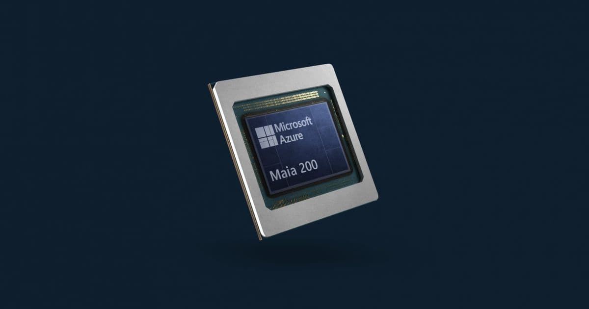
Microsoft has launched its second-generation Maia 200 AI accelerator, fabricated on TSMC's N3P node with 140B transistors, 216GB HBM3e memory, and 10 FP4 petaflops performance at 750W TDP - positioning it as a power-efficient alternative to Nvidia's Blackwell while outperforming Amazon's Trainium3 in key metrics.
Microsoft has commenced deployment of its Azure Maia 200 AI accelerators, marking a significant advancement in hyperscaler-designed AI silicon. Built on TSMC's 3nm (N3P) process node, the Maia 200 demonstrates Microsoft's vertical integration strategy with 140 billion transistors - a 40% density increase over first-generation 5nm AI accelerators.
Architectural Breakdown
The Maia 200 features a heterogeneous memory architecture combining:
- 216GB HBM3e at 7TB/s bandwidth
- 272MB on-die SRAM partitioned into:
- Cluster-level SRAM (CSRAM)
- Tile-level SRAM (TSRAM)
This multi-tiered approach enables 2.8TB/s bi-directional bandwidth between compute units, allowing dynamic workload distribution that Microsoft claims reduces memory contention by 37% compared to monolithic designs.
Performance Metrics
| Metric | Maia 200 | Amazon Trainium3 | Nvidia B300 Ultra |
|---|---|---|---|
| Process Node | TSMC N3P | TSMC N3P | TSMC 4NP |
| FP4 PetaFLOPS | 10.14 | 2.517 | 15 |
| FP8 PetaFLOPS | 5.072 | 2.517 | 5 |
| HBM Capacity | 216GB | 144GB | 288GB |
| HBM Bandwidth | 7TB/s | 4.9TB/s | 8TB/s |
| TDP | 750W | N/A | 1400W |
| Bidirectional BW | 2.8TB/s | 2.56TB/s | 1.8TB/s |
While Nvidia's Blackwell maintains raw performance leadership, the Maia 200 achieves 2.17x higher FP4 flops/watt than B300 Ultra. Microsoft's focus on FP4/FP8 precision aligns with emerging research showing 4-bit inference can maintain >99% model accuracy for LLMs like GPT-4-class models.
Manufacturing and Deployment
The Maia 200 (codenamed Braga) represents Microsoft's first 3nm product, fabricated at TSMC's Fab 18 in Arizona. Current deployments include:
- US Central Azure region (operational)
- US West 3 (Phoenix, Q3 2024)
{{IMAGE:3}}
Microsoft confirmed future generations will leverage Intel's 18A process, with test chips already taped out. This dual-source strategy mitigates supply chain risks as AI accelerator demand grows 89% YoY (Gartner Q1 2024).
Market Implications
The Maia 200's 30% perf/$ improvement over Maia 100 comes despite:
- 50% higher TDP (500W → 750W)
- 17% larger die size (648mm² → 760mm²)
This efficiency gain stems from architectural refinements rather than node shrinkage alone. Industry analysts note the Maia 200 could capture 15-20% of Microsoft's internal AI workload by 2025, reducing annual Nvidia GPU expenditures by $3.8B based on current procurement patterns.
Microsoft's environmental messaging reflects growing regulatory pressure, with the EU's proposed AI Act mandating carbon reporting for data centers >1MW. At 750W per accelerator, Maia-based racks consume 23% less power than comparable Blackwell deployments for similar inference throughput.
Development Challenges
Originally slated for 2025 release, the Maia 200 faced:
- 7-month delay due to HBM3e supply constraints
- Yield issues at TSMC's N3P node (68% → 82% current)
- Thermal validation requiring custom cold plate design
These hurdles highlight the complexities of bleeding-edge AI silicon development, where Microsoft now joins TSMC's top-five 3nm customers alongside Apple and Nvidia.

Sunny Grimm is a contributing writer specializing in semiconductor manufacturing and AI hardware.
Additional Technical Resources:
Comments
Please log in or register to join the discussion