A hardware modder has engineered a unique Turing-era graphics card by transplanting a fully unlocked Titan RTX core and 24GB of memory onto an RTX 2080 Ti Hall of Fame PCB, pushing the power limit to 900W and achieving a 3DMark TimeSpy Extreme score that surpasses dual Titan RTX setups.
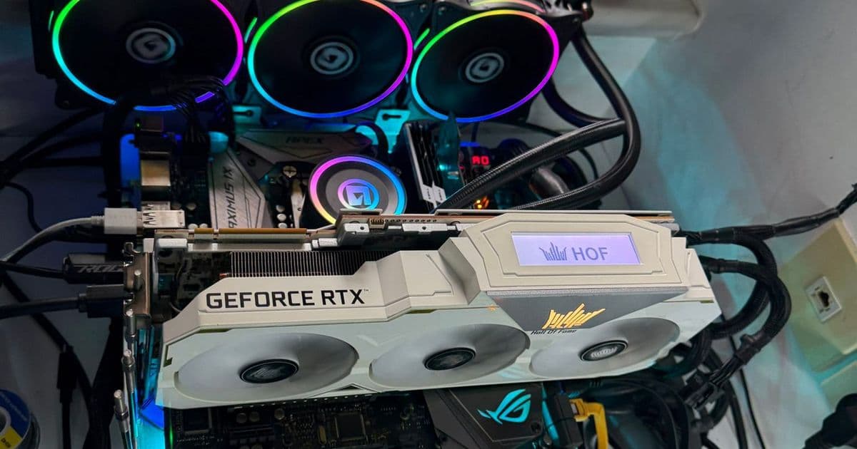
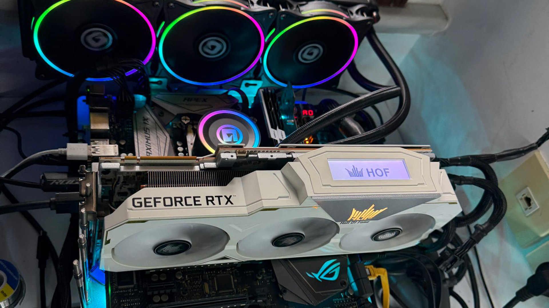
A hardware modification project has demonstrated the latent potential within Nvidia's Turing architecture by creating a hybrid graphics card that merges the best of two different GPU models. Modder Jiachen Liu, known on X as @unnatural__log, has successfully transplanted the fully unlocked GPU core from an RTX Titan onto a Galax RTX 2080 Ti Hall of Fame (HoF) printed circuit board (PCB), resulting in a unique, single-GPU powerhouse.
The core of this modification addresses a fundamental limitation in Nvidia's product segmentation strategy. The consumer-focused RTX 2080 Ti, while powerful, shipped with its TU102 silicon partially disabled. It featured 68 Streaming Multiprocessors (SMs), totaling 4,352 CUDA cores, and a 352-bit memory interface connected to 11GB of GDDR6 memory. In contrast, the professional-grade RTX Titan utilized the same TU102 die but with all 72 SMs enabled, unlocking 4,608 CUDA cores and a full 384-bit bus paired with 24GB of GDDR6 memory.
Liu's mod bridges this gap by physically removing the GPU die and memory modules from a donor Titan RTX and soldering them onto the HoF 2080 Ti's PCB. This is not a simple software unlock; it's a physical transplant that grants the modified card the full hardware specifications of the Titan RTX. The result is a card with 4,608 CUDA cores and 24GB of memory on a 384-bit interface, but with a critical advantage: the superior power delivery and cooling potential of the 2080 Ti HoF board.
The Galax RTX 2080 Ti HoF is renowned in the enthusiast community for its robust 16+3 phase power delivery system and a massive triple-fan cooler. Nvidia's reference Titan RTX board, by comparison, was designed for stability and professional workloads rather than extreme overclocking. By placing the Titan core on the HoF PCB, Liu gained access to a much higher power budget. He modified the card's power limit from the Titan's 280W to a staggering 900W, allowing for significantly higher sustained clock speeds.
The performance results validate the approach. Under this new configuration, the modified card achieved a graphics score of 18,038 in 3DMark TimeSpy Extreme, a demanding benchmark that stresses both GPU compute and memory bandwidth. To contextualize this figure: an average score for two Titan RTX cards running in SLI (NVIDIA's multi-GPU technology) is approximately 17,000 points. A single, stock RTX 3090 scores around 14,000 points in the same test. The modded card's single-GPU score effectively outperforms a dual-Titan RTX setup, showcasing the impact of the unlocked hardware and the massive power envelope.
Furthermore, Liu reported that the HoF cooler and power system enabled a sustained core clock of 2,150 MHz. This level of frequency is exceptionally difficult to maintain on the stock Titan RTX due to its more conservative thermal and power design. The modification effectively creates a "best of both worlds" product: the fully unlocked silicon of the Titan RTX combined with the overclocking-focused engineering of a top-tier 2080 Ti custom model.
This project highlights several key aspects of semiconductor design and market segmentation. First, it underscores that the performance differences between consumer and prosumer/professional products are often not due to physical limitations of the silicon itself, but rather intentional binning and firmware restrictions. The same TU102 die can operate at vastly different performance levels based on how many units are enabled and the power budget allowed.
Second, it demonstrates the importance of the printed circuit board (PCB) and power delivery subsystem in unlocking a GPU's potential. The GPU die is only one component; the surrounding infrastructure that supplies stable power and dissipates heat is equally critical for high performance. The modder's choice of the HoF PCB was deliberate, as it provided the necessary foundation to handle the 900W power target and maintain high clock speeds.
The project also serves as a fascinating case study in the Turing architecture's capabilities. The TU102 die, now several generations old, still possesses significant computational power, especially when fully enabled and given ample power. The resulting performance, while achieved under extreme conditions, shows that the architectural foundations of Turing remain potent, particularly for memory-intensive workloads thanks to the expanded 24GB frame buffer.
While this is a one-off modding project, it illustrates the untapped potential that often exists within commercial silicon. For enthusiasts and engineers, it's a reminder that the specifications on a product page represent a carefully calibrated balance of performance, cost, and market positioning, not necessarily the absolute physical limits of the hardware.
Images of the modification process and benchmark results can be found on the modder's X post: https://twitter.com/unnatural__log/status/1882372268086542592
Comments
Please log in or register to join the discussion