
Glass interposers promise denser interconnects, less warping, and 448 Gbps signal integrity for AI accelerators. The catch is a 70 percent manufacturing yield that has to climb before any of it ships at volume.
Semiconductor packaging rarely makes headlines, which is part of why the current push toward glass substrates is easy to miss. The chips themselves get the attention. But for AI accelerators and the high-bandwidth memory stacks that feed them, the material sitting underneath the silicon has quietly become a limiting factor. Intel has put more than $1 billion behind glass as a replacement for the organic substrates that have carried the industry for about 25 years, and Samsung, Absolics, DNP, Unimicron, LG Innotek, and TOPPAN are all working the same problem from different angles.
What's claimed
The pitch is that glass substrates and glass interposers solve several problems that organic materials cannot, all at once: less mechanical warping, denser interconnects, cleaner high-frequency signals, and better power delivery. Intel has shown 448 Gbps signal integrity on a glass substrate, which is the headline number most coverage leads with. The broader claim is that as AI packages keep growing in area and pin count, organic substrates are running out of room to scale, and glass is the next workhorse.
That framing is mostly accurate, which is worth saying up front because packaging announcements often overstate how close a technology is to production. The physics here is real and the problems being solved are specific rather than vague.
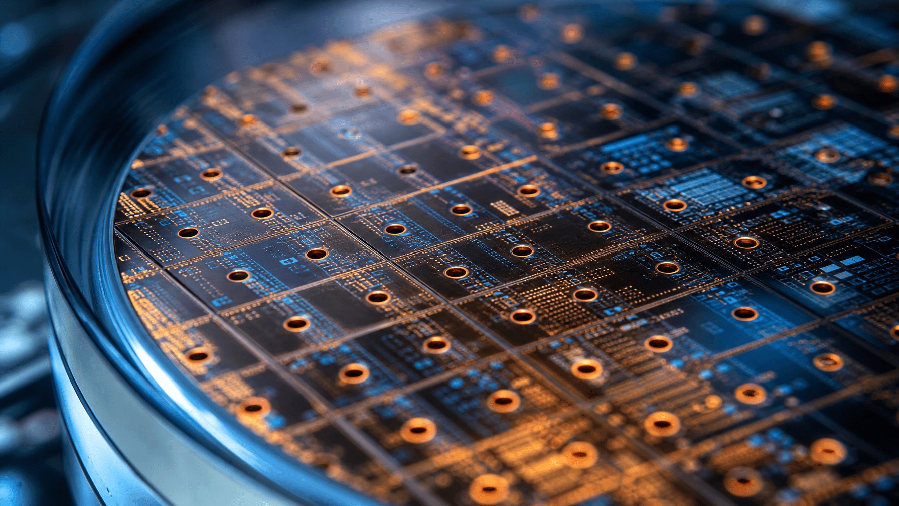
What's actually new
The core issue with organic substrates is coefficient of thermal expansion, or CTE. Organic materials expand at roughly 17 to 20 parts per million per degree Celsius. Silicon expands at about 3 ppm per degree Celsius. When you bond a large silicon die to a substrate that expands six times faster as the package heats up, the two materials fight each other. On small packages this is manageable. On the large packages that modern AI accelerators require, the mismatch produces warping that hurts reliability and yields, and it gets worse as die area grows. Glass can be formulated to sit much closer to silicon's expansion rate, which removes a large source of mechanical stress rather than just managing it.
Interconnect density is the second lever. Vias in organic substrates are made by mechanical drilling, which bottoms out at around 100 micrometers in diameter. Glass is laser-drilled, and the practical via diameter drops to somewhere in the 10 to 30 micrometer range. That is a roughly three-to-tenfold improvement in how tightly you can pack vertical connections, which translates directly into more routing between the die and the rest of the system. For designs that stitch together multiple compute chiplets and several HBM stacks on one package, that headroom matters.
Signal integrity benefits from a more mundane property: glass is smooth. Rough organic surfaces scatter and attenuate high-frequency signals through what is called the skin effect, where current crowds toward the conductor surface at high frequencies and surface roughness raises losses. A flatter, smoother dielectric lowers that loss, which is the mechanism behind the 448 Gbps demonstration. Power integrity improves for a related reason, because uniform laser-drilled vias deliver more consistent current paths than the uneven via sizing organic processes tend to produce.
None of these are incremental tweaks to an existing material. They come from switching the substrate material entirely, which is why the investment numbers are large and the timelines are measured in years.
Limitations
The gap between a demonstration and a shipping product is manufacturing yield, and this is where glass is not ready. Current glass substrate yields sit around 70 percent. Organic substrates reliably clear 90 percent and have decades of process maturity behind them. A 20-point yield gap on an expensive, large-area part is not a rounding error. It is the difference between a viable cost structure and one that only works for the most margin-rich products.
The specific process steps that need work are dicing, via filling, and surface flatness. Glass is brittle, so singulating panels into individual substrates without introducing micro-cracks is harder than cutting organic laminate. Filling those narrow laser-drilled vias with conductor uniformly, without voids, is its own challenge at 10 to 30 micrometers. And maintaining flatness across a large panel is exactly the property that makes glass attractive, so any process that warps or stresses the panel undercuts the reason to use it.
There is also a structural point about who is building this. Absolics, the U.S. company constructing a dedicated facility in Georgia, is backed by CHIPS Act funding, and Samsung is leaning on its display-glass manufacturing to bootstrap a vertically integrated approach. Intel's glass substrate research is the most publicly detailed, but a demonstration from a research line is not the same as high-volume production. The fact that so many players are entering at once signals genuine opportunity, and it also signals that nobody has locked in a process that clearly wins yet.
Why it matters
For anyone tracking where AI compute cost goes, packaging is an increasingly large share, and the substrate is part of that. If glass delivers on density and warping while closing the yield gap, it removes a ceiling that organic materials are bumping against as accelerator packages keep growing. The likeliest path is that glass shows up first in the highest-end AI and data center parts, where the performance gains justify the cost premium and lower yield, and migrates downward only as the process matures. The technology is credible. The schedule depends almost entirely on whether 70 percent yield can become 90 percent, and that is a manufacturing question, not a physics one.
Comments
Please log in or register to join the discussion