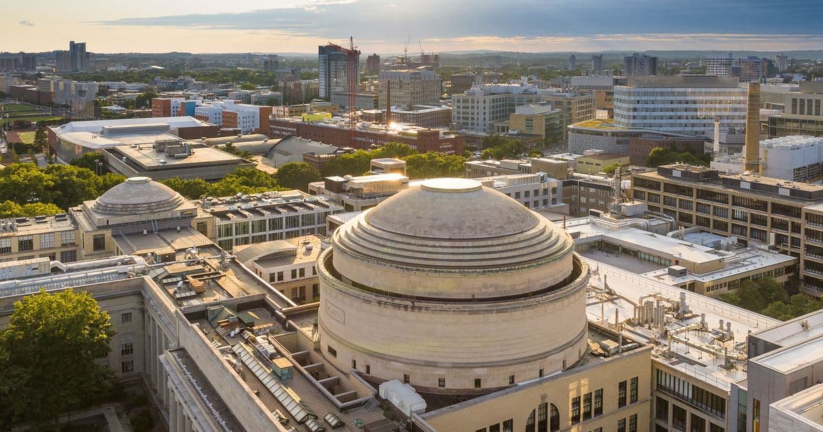
MIT’s new Quantum Systems Laboratory, backed by state and federal funds, will provide shared quantum hardware, sensors and interconnects to academia, government and industry, positioning Massachusetts as a hub for next‑generation quantum technologies.
MIT’s Quantum Systems Laboratory opens a shared‑use quantum hub
On May 28, MIT President Sally Kornbluth and Massachusetts Governor Maura Healey announced the creation of the Quantum Systems Laboratory (QSL), a dedicated facility that will bring together a superconducting quantum processor, cryogenic testbeds, quantum‑grade sensors and high‑bandwidth interconnects under one roof. The lab will sit in Building 39 and be open to researchers from MIT, the University of Massachusetts system, Harvard, federal labs and private firms.
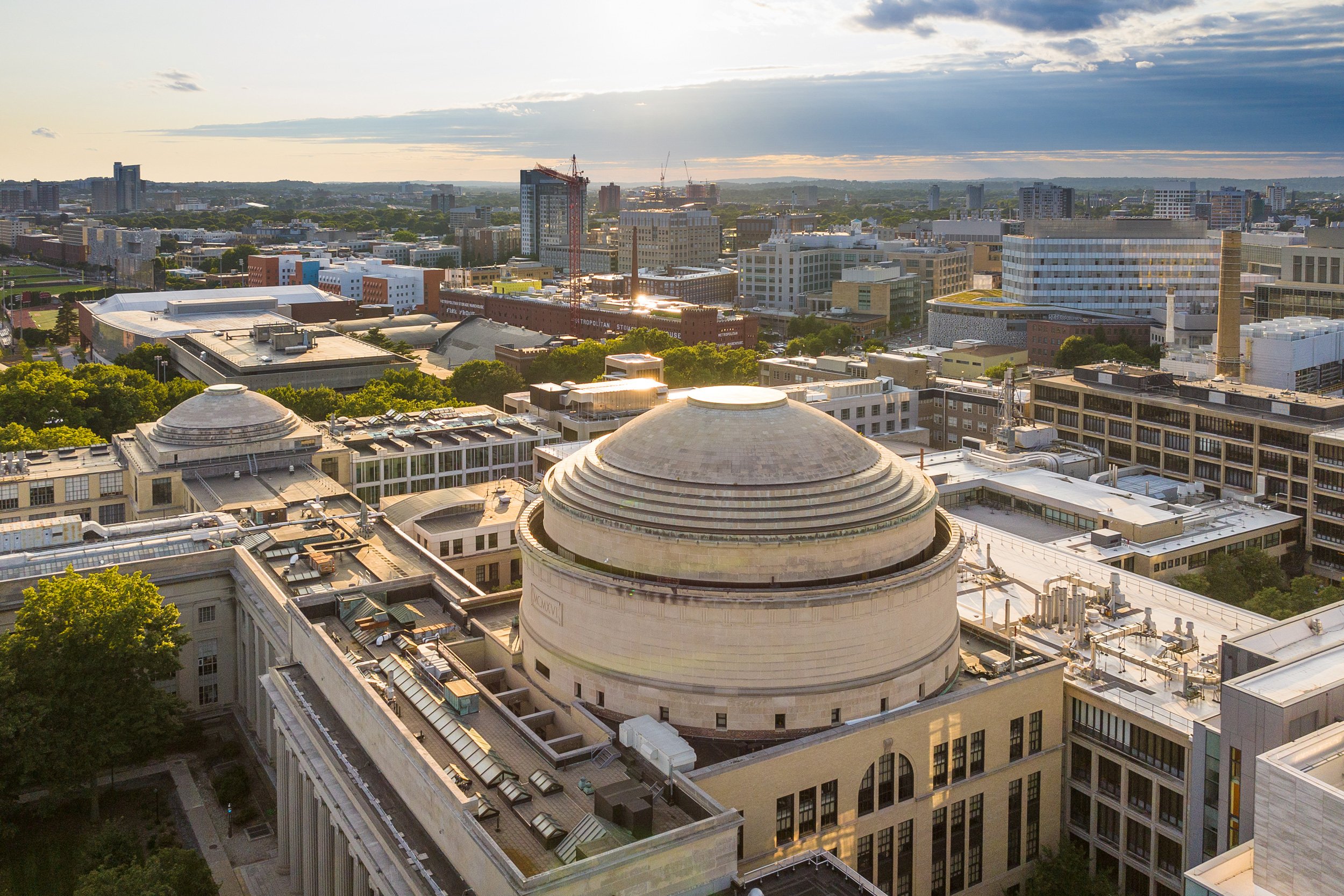
Technical approach: a modular quantum toolbox
QSL is designed around a modular architecture that mirrors the emerging industry practice of separating the quantum processor (“the qubit chip”) from the surrounding control and readout stack. The core of the lab is a dilution‑refrigerator platform capable of reaching temperatures below 10 mK, which will host a 64‑qubit superconducting processor supplied by a partnership with a leading vendor. Around this processor, the lab will house:
- Quantum interconnect racks – microwave and optical links that enable coherent transfer of quantum states between separate chips, a capability needed for scaling beyond a single processor.
- Cryogenic sensor suites – single‑photon detectors, nano‑SQUID magnetometers and optomechanical resonators that can be used for precision metrology, dark‑matter searches and biomedical imaging.
- Control electronics pods – FPGA‑based arbitrary waveform generators and low‑noise amplifiers that operate at both room temperature and cryogenic stages, allowing researchers to prototype custom pulse sequences without building their own hardware.
- Clean‑room micro‑fabrication bays – a small‑scale fab for rapid prototyping of superconducting circuits, ion‑trap chips and photonic waveguides, linked to the existing MIT.nano facilities for more advanced processing.
The modular layout lets a team focused on, say, quantum sensing, plug their device into the same cryogenic bus that a quantum‑computing group uses for algorithm testing. This shared‑use model reduces duplication of expensive infrastructure and accelerates cross‑disciplinary experiments.
Real‑world applicability and early use cases
The lab’s first wave of projects targets three high‑impact domains:
- Secure communications – Researchers will test quantum key distribution (QKD) protocols over fiber and free‑space links using the lab’s optical interconnects, aiming for field‑ready transceivers that can be deployed by the U.S. Department of Defense.
- Materials discovery – By coupling the quantum processor to a variational quantum eigensolver (VQE) workflow, chemists will explore catalytic pathways for carbon‑neutral fuel synthesis, shortening the design cycle from months to weeks.
- Quantum‑enhanced navigation – The cryogenic sensor suite will be used to develop atom‑interferometer gyroscopes that can operate without GPS, a capability of interest to autonomous vehicle manufacturers and aerospace firms.
Because the facility is open to government labs, startups, and academic groups, a company developing a quantum‑ready encryption chip can test its hardware on the same refrigerator that a university team uses for fundamental physics experiments. This reduces the time‑to‑market for commercial products and gives students hands‑on experience with production‑grade equipment.
Funding, timeline and broader impact
The Commonwealth is contributing $25 million, matching a portion of existing federal grants that support MIT’s quantum research portfolio. Construction is slated to begin this summer, with the first operational cryogenic bays expected in early 2027. In addition to the direct 150+ construction jobs, the lab is projected to create 75–100 permanent research and support positions across the region.
Beyond jobs, QSL strengthens the quantum talent cluster that already includes MIT.nano, the Lincoln Laboratory SQUILL foundry, and dozens of spin‑out companies. By providing a shared, high‑performance testbed, the lab lowers the barrier for smaller firms and university labs to experiment with quantum hardware, a critical step toward a sustainable quantum ecosystem.
For more details on the facility’s technical specifications, see the official MIT announcement here.
Comments
Please log in or register to join the discussion