MIT researchers have developed a new class of photonic chips with microscopic structures that curl upward like ski jumps, enabling precise control of thousands of laser beams in free space for applications in high-resolution displays, compact Lidar systems, and large-scale quantum computers.
Researchers from MIT and collaborators have unveiled a breakthrough in photonic chip technology that could transform how we interact with light-based computing systems. Their new platform, featuring microscopic structures that curl upward like tiny ski jumps, enables precise control of thousands of laser beams simultaneously, opening doors to applications ranging from ultra-high-resolution displays to larger quantum computers.
The Challenge of Free-Space Light Control
Traditional photonic chips excel at processing data using light instead of electricity, offering faster communication speeds and greater bandwidth. However, most light remains trapped within the chip's optical wiring, making it difficult to efficiently transmit to the outside world. This limitation has constrained applications that require precise control of light in free space.
"On a chip, light travels in wires, but in our normal, free-space world, light travels wherever it wants," explains Henry Wen, visiting research scientist at MIT's Research Laboratory of Electronics. "Interfacing between these two worlds has long been a challenge."
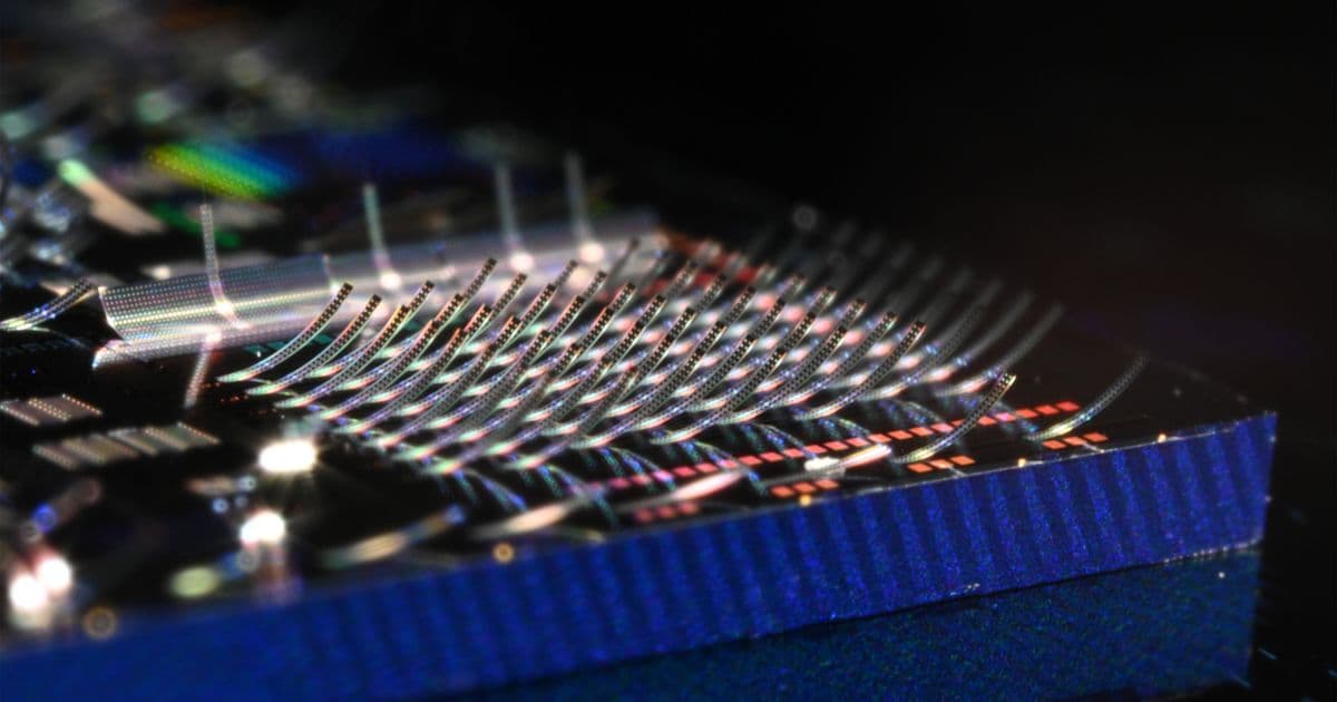
The Ski Jump Solution
The MIT team's innovation centers on a new fabrication technique that creates microscopic structures curving upward off the chip's surface. These "ski jump" structures are built using two-layer materials—silicon nitride and aluminum nitride—that expand differently when cooling from high fabrication temperatures. By designing special patterns in each layer, the researchers exploit thermal strain to make the entire structure curl upward as it cools.
This approach, inspired by old-fashioned thermostats that use bimetallic coils, produces thousands of individually controllable laser beams that can interact with the world outside the chip in a single shot.
Precision Control at Scale
The platform's true power lies in its scalability. While existing methods for broadcasting and steering light off photonic chips typically work with only a few beams at once, the MIT team's system can control thousands simultaneously. Connected waveguides funnel light to the ski jump structures, while modulators rapidly and precisely control when each beam turns on and off.
"We can't control a million laser beams, but we may need to control a million qubits," Wen notes, explaining the technology's origins in the Quantum Moonshot Program—a collaboration between MIT, the University of Colorado at Boulder, MITRE Corporation, and Sandia National Laboratories to develop diamond-based quantum computing platforms.
Painting with Light
By broadcasting light in different colors and adjusting light frequencies, the researchers can essentially "paint" pictures in free space. The system's stability is remarkable—patterns remain perfectly still without requiring error correction. The researchers simply calculate which color lasers need to be on at a given time and activate them.
This capability enables extremely high-resolution displays. Where smartphone displays might fit two pixels in a given area, the MIT team's technique can accommodate 30,000 pixels in the same space. "Our platform is the ideal optical engine because our pixels are at the physical limit of how small a pixel can be," Wen says.
Beyond Displays
The technology's potential extends far beyond high-resolution screens. For quantum computing, the ability to control millions of qubits simultaneously using laser beams could enable significantly larger quantum systems. The platform could also produce Lidar systems small enough to fit on tiny robots, or dramatically accelerate 3D printing processes that use lasers to cure resin layers.
Looking Ahead
While the current research demonstrates the technology's capabilities, the team plans to scale up the system and conduct additional experiments on yield and uniformity. They aim to design larger systems that capture light from arrays of photonic chips with ski jumps and perform robustness tests to evaluate device longevity.
"We envision this opening the door to a new class of lab-on-chip capabilities and lithographically defined micro-opto-robotic agents," Wen says.
The research, published today in Nature, represents a significant step toward bridging the gap between on-chip photonic processing and free-space light applications. By solving the long-standing challenge of efficiently beaming light from photonic chips into the surrounding environment, the MIT team has created a platform with far-reaching implications for computing, display technology, and quantum information processing.
The work was funded by the MITRE Quantum Moonshot Program, the U.S. Department of Energy, and the Center for Integrated Nanotechnologies, highlighting the collaborative nature of this fundamental advance in photonic technology.
Comments
Please log in or register to join the discussion