A Bill Gates-backed startup is developing a massive optical systolic array that promises 10x the performance of Nvidia's latest GPUs for the same power, but the technology is years away from production and faces significant engineering hurdles.
The slowdown of Moore's Law has chip designers scrambling for alternatives, and one of the more audacious approaches comes from Neurophos, an Austin-based startup that has secured $110 million in Series-A funding led by Gates Frontier. The company is betting on optical transistors—specifically, micron-scale metamaterial modulators—to deliver what its CEO Patrick Bowen claims is a 10x performance advantage over Nvidia's newly unveiled Rubin GPUs for AI inference workloads, all while consuming roughly the same amount of power.
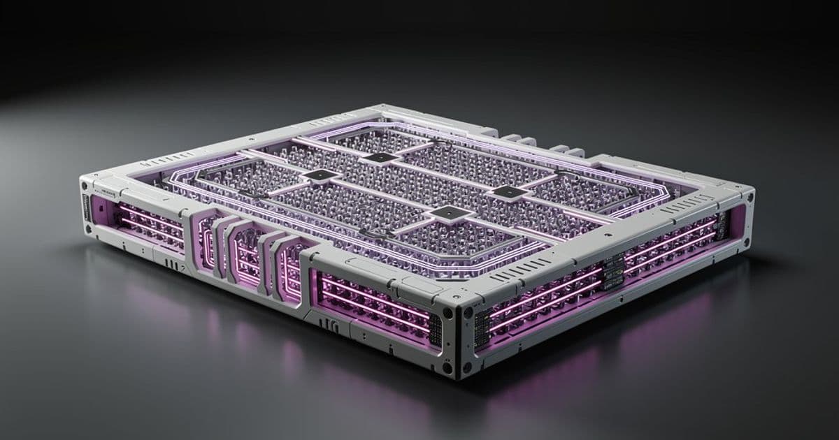
At the heart of Neurophos's approach is a single, massive photonic tensor core. Unlike conventional AI accelerators that pack dozens or even hundreds of smaller tensor cores onto a chip, Neurophos's first-generation optical processing unit (OPU), codenamed Tulkas T100, features just one core. This core is a 1,000 by 1,000 array of processing elements—significantly larger than the 256x256 arrays found in most current AI accelerators. The core operates at 56GHz, but because the matrix multiplication is performed optically, the power consumption is primarily limited to the energy required for opto-electrical conversion.
The key innovation here is the optical transistor itself. Traditional silicon photonics produces optical modulators that are roughly 2mm long, which severely limits compute density. Neurophos claims to have shrunk these components by a factor of 10,000, achieving micron-scale dimensions that are compatible with standard CMOS manufacturing processes. This density breakthrough, Bowen says, is what makes the massive systolic array feasible.
The Tulkas T100 is designed as a dual reticle chip with 768GB of HBM memory, targeting 470 petaFLOPS of FP4/INT4 compute at 1-2 kilowatts of power. For context, Nvidia's Rubin GPUs are expected to deliver around 50 petaFLOPS of FP4 performance, making Neurophos's claims substantial if realized. However, these figures represent target specifications rather than proven benchmarks. The chip is still in active development, with full production not expected until mid-2028, and Bowen anticipates initial volumes in the thousands rather than tens of thousands of units.
The company's initial focus is on the prefill phase of large language model inference—the compute-intensive stage where input tokens are processed. This aligns with a growing industry trend toward disaggregating inference workloads. Nvidia has already introduced its Rubin CPX as a dedicated prefill accelerator, and Neurophos envisions its Tulkas T100 serving a similar role. Bowen's long-term vision involves pairing one rack of Neurophos chips (256 units) with an NVL576 rack system for comprehensive inference acceleration.
However, significant challenges remain. The decode phase of inference—generating output tokens—is memory bandwidth-bound rather than compute-bound, and Neurophos acknowledges that technologies like co-packaged optics will need to mature before they can address this stage. Additionally, the company's approach requires substantial supporting infrastructure: the 25mm² tensor core occupies only a fraction of the reticle-sized die, with the remainder dedicated to vector processing units and SRAM to prevent data starvation.
The broader context for Neurophos's approach is the increasing energy demands of AI compute. As Bowen notes, the industry is reaching physical limits with traditional CMOS scaling, and optical computing offers a potential path forward. The company's proof-of-concept chip, currently in development with the new funding, will be crucial in validating whether these theoretical advantages translate to real-world performance.
Skeptics point out that optical computing has been "just around the corner" for decades, and the challenges of integration, manufacturing consistency, and software ecosystem development are substantial. Broadcom's CEO recently stated that silicon photonics won't matter "anytime soon," reflecting industry caution. Yet the Gates-backed funding suggests at least some investors believe the timing might finally be right.
The success of Neurophos's approach will depend not just on the optical transistors themselves, but on the entire system architecture. The massive tensor core requires sophisticated data movement and memory management, and the software stack will need to be optimized for this unconventional architecture. If successful, it could represent a meaningful departure from the incremental improvements that have characterized chip design in recent years.
For now, Neurophos remains a high-risk, high-reward bet on optical computing's potential to break through the constraints of traditional semiconductor scaling. The company's progress over the next few years will be closely watched as a test case for whether optical transistors can indeed bend Moore's Law back toward its historical trajectory.
Comments
Please log in or register to join the discussion